Module 6: Hardening Your Design for the OpenFrame Multi-Project
Table of Contents
1. OpenFrame — The Bare Padframe Platform
OpenFrame is an alternative chip harness to Caravel. Where Caravel includes a full management SoC, a Wishbone bus, and a logic analyser, OpenFrame provides only the essential harness — a padframe, a power-on-reset circuit, and a 32-bit project ID ROM.
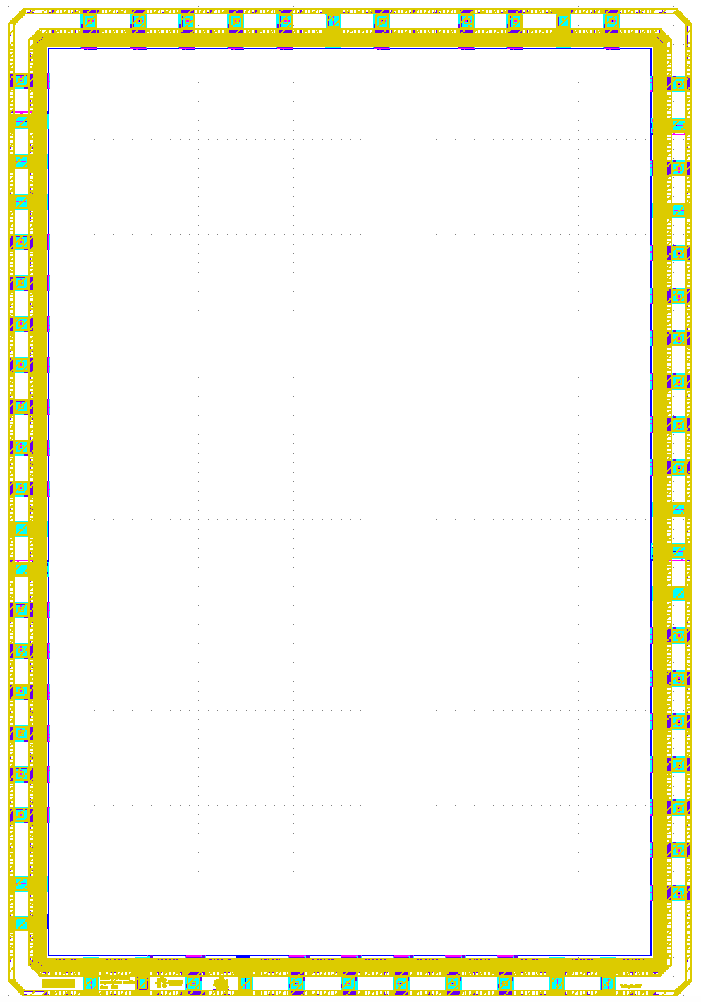
Fig. 36 OpenFrame chip — bare padframe with a ~15 mm² open user area. All 44 GPIO pads are directly accessible by the user design with no SoC intermediary.
This minimal footprint gives you maximum freedom:
Caravel |
OpenFrame |
|
|---|---|---|
Management SoC |
✅ PicoRV32 + peripherals |
❌ None |
Wishbone bus |
✅ Required for host access |
❌ Not available |
GPIO access |
Shared with SoC |
Full direct control |
User area |
~10 mm² |
~15 mm² |
Interface protocol |
Wishbone registers |
Any — you design it |
I/O Frame Only
OpenFrame provides only the pad ring (GPIO and power pads) and the flat power grid. Everything inside the user area is user-defined. There is no CPU, no bus protocol, and no firmware — your design is directly responsible for all GPIO configuration and control.
Because there is no management SoC, you do not need a Wishbone wrapper around your
design. Your logic connects directly to the GPIO pads through the pin interface of the
project_macro boundary.
2. The AUC Silicon Sprint Multi-Project Chip
The AUC Silicon Sprint does not dedicate the entire OpenFrame user area to a single design. Instead, the chip is partitioned to host up to 12 independent student projects in a single fabrication run, arranged in a 4-row × 3-column grid.

Fig. 37 OpenFrame Multi-Project floorplan — 4 rows × 3 columns of project slots. Each slot is connected to the GPIO padframe through dedicated orange mux macros.
A scan-chain-configurable MUX tree routes the chip’s 38 usable GPIOs to exactly one selected project at runtime. When a project is activated, its three orange mux macros (bottom, right, and top) connect it to the physical pads. All other projects remain electrically isolated.
Each project slot communicates with the outside world through the project_macro
boundary ports:
Edge |
Signals |
Route to pads |
|---|---|---|
Left |
|
From the green macro (chip-wide clock and reset distribution) |
Bottom |
|
Via bottom orange mux → right-side GPIO pads |
Right |
|
Via right orange mux → top-side GPIO pads |
Top |
|
Via top orange mux → left-side GPIO pads |
Total usable GPIOs per project: 15 + 9 + 14 = 38.
The orange muxes, green macro, purple routing macros, and scan controller are all
pre-hardened fixed infrastructure. You do not touch them. Your responsibility is
to harden your own project_macro to the correct footprint and submit the GDSII.
For a deeper understanding of the system architecture and the multiproject environment, please refer to the following resource:
OpenFrame Multiproject Documentation: Caravel OpenFrame MPC Overview
3. Design Rules and Integration Contract
Before writing a single line of RTL, understand the constraints that the multi-project chip imposes on every participating macro. Violating any of these will prevent your design from being integrated.
Fixed-Budget Chip Resources
The die area is fixed. Power, I/O pads, clock, and layer usage must all be budgeted up front across every participating macro. You share the chip with up to 11 other students — your choices affect everyone.
What You Must Follow
Constraint |
Rule |
Reason |
|---|---|---|
Die area |
Fixed at |
Every slot is placed at pre-determined coordinates. A different size breaks the assembly. |
RTL interface |
Use the exact port list of the |
This port list is the black box used at the top level. Any change to it breaks connectivity. |
DEF template |
Use |
Pin locations and power ring geometry are fixed by the top-level integration. |
PDN configuration |
Use |
Metal 5 is reserved for the top-level power straps. Any Metal 5 geometry inside your macro creates a DRC short that blocks the power delivery to adjacent projects. |
Routing layer cap |
Use |
Same reason as above — Metal 5 must remain clear for the wrapper’s power straps to pass through. |
Power domain |
Use |
The slot’s power is connected by the top-level wrapper. You declare the nets; the top level provides the connections. |
Clock port |
Use port name |
The green macro drives |
Timing constraints |
Use the The Retrieved Constraints part. |
These encode the measured electrical delays through openframe. |
Note
If you use PDN_CORE_RING: true or allow Metal 5 routes, the resulting obstructions
will block the top-level Metal 5 straps from reaching the other projects in the grid.
The error cannot be fixed after integration — it would require re-running your macro.
4. The project_macro Slot
Each student’s design occupies a single project slot with a fixed physical footprint of 880 × 1031.66 µm. All 12 slots in the chip are identical in size and pin placement.
We provides a DEF template for the slot. LibreLane uses this template at the floorplan step to stamp the exact boundary, I/O pin locations, and power ring geometry into your design database — guaranteed to match what the top-level integration expects.
Use the Template DEF As-Is
Do not modify fixed_dont_change/project_macro.def. It contains the exact pin positions
and power ring that the surrounding orange and green macros connect to. Any change —
even a single pin shifted by one grid step — will produce a DRC violation or unconnected
net when your macro is placed in the chip.
5. Workshop Repository & File Structure
Clone the workshop repository:
$ git clone https://github.com/basemhesham/openframe_multiproject ~/openframe_multiproject
The relevant directory structure is:
~/openframe_multiproject/
├── verilog/
│   └── rtl/
│       └── project_macro.v          ← Template — add your design here
├── openlane/
│   └── project_macro/
│       ├── config.json              ← Hardening configuration (edit this)
│       ├── fixed_dont_change/
│       │   └── project_macro.def   ← Fixed slot DEF template — do NOT edit
│       ├── pnr.sdc                  ← PnR timing constraints
│       └── signoff.sdc              ← Signoff timing constraints
6. Integrating Your Design into project_macro
Open the template file:
$ gedit ~/openframe_multiproject/verilog/rtl/project_macro.v
The template declares the complete port list that the chip infrastructure connects to.
Do not change the module name or any port declaration. Replace the tie-off logic
inside the USER LOGIC GOES HERE section with your own design — either by
instantiating a submodule or by writing your RTL directly.
project_macro.v — Template
// SPDX-License-Identifier: Apache-2.0
// project_macro — User design sandbox
//
// Port mapping by physical edge:
//   Left:   clk, reset_n (from green macro)
//   Bottom: 15 GPIOs (-> bottom orange -> Caravel right pads)
//   Right:  9 GPIOs  (-> right orange  -> Caravel top pads)
//   Top:    14 GPIOs  (-> top orange    -> Caravel left pads)
//
// Total usable GPIOs: 15 + 9 + 14 = 38
// All outputs have safe default tie-offs. Users replace them with their logic.
//
// GPIO Signal Reference:
//   gpio_*_out : Data driven onto the pad (active when oeb=0)
//   gpio_*_oeb : Output Enable Bar (0=output, 1=input/Hi-Z)
//   gpio_*_in  : Data sampled from the pad (always available)
//   gpio_*_dm  : Drive Mode, 3 bits per pad [dm2, dm1, dm0]
//
// Drive Mode (dm[2:0]) — Sky130 OpenFrame GPIO Pad Modes:
//   3'b000 : High-Z / Analog mode (pad completely disconnected)
//   3'b001 : Input only, no pull resistor
//   3'b010 : Input with weak pull-down (~50kΩ to VSS)
//   3'b011 : Input with weak pull-up   (~50kΩ to VDD)
//   3'b100 : Slow-slew output (reduced dI/dt for noise-sensitive signals)
//   3'b101 : Slow-slew output with open-drain (external pull-up required)
//   3'b110 : Strong digital push-pull output (DEFAULT — standard digital I/O)
//   3'b111 : Strong digital output with weak pull-up
//
// Note: oeb controls the output driver gate. dm configures the pad cell itself.
//   - For pure input:  oeb=1, dm=3'b001 (or 3'b010/011 for pull-down/up)
//   - For push-pull:   oeb=0, dm=3'b110
//   - For open-drain:  oeb=0, dm=3'b101 (needs external pull-up)
//   - For analog:      oeb=1, dm=3'b000 (bypasses digital buffers entirely)

`default_nettype none

module project_macro (
`ifdef USE_POWER_PINS
    inout vccd1,
    inout vssd1,
`endif
    // From green macro (left edge)
    input  wire        clk,
    input  wire        reset_n,
    input  wire        por_n,

    // Bottom GPIOs (15) -> Caravel right pads via bottom orange chain
    input  wire [14:0] gpio_bot_in,
    output wire [14:0] gpio_bot_out,
    output wire [14:0] gpio_bot_oeb,
    output wire [44:0] gpio_bot_dm,

    // Right GPIOs (9) -> Caravel top pads via right orange chain
    input  wire [8:0]  gpio_rt_in,
    output wire [8:0]  gpio_rt_out,
    output wire [8:0]  gpio_rt_oeb,
    output wire [26:0] gpio_rt_dm,

    // Top GPIOs (14) -> Caravel left pads via top orange chain
    input  wire [13:0] gpio_top_in,
    output wire [13:0] gpio_top_out,
    output wire [13:0] gpio_top_oeb,
    output wire [41:0] gpio_top_dm
);

    // ============================================================
    // USER LOGIC GOES HERE — Replace the safe tie-offs below
    // ============================================================

    // Safe defaults: all pads configured as inputs (oeb=1) driving zero.
    // Even if accidentally enabled, outputs are low — no floating or
    // contention risk. dm=3'b110 (strong push-pull) is chosen so that
    // when a project IS selected, its pads are ready for digital I/O
    // without needing to reconfigure dm via the scan chain.

    // Bottom: 15 GPIOs, all input
    assign gpio_bot_out = 15'b0;
    assign gpio_bot_oeb = {15{1'b1}};

    // Right: 9 GPIOs, all input
    assign gpio_rt_out = 9'b0;
    assign gpio_rt_oeb = {9{1'b1}};

    // Top: 14 GPIOs, all input
    assign gpio_top_out = 14'b0;
    assign gpio_top_oeb = {14{1'b1}};

    // Drive mode: 3'b110 = strong digital push-pull (see mode table above)
    genvar i;
    generate
        for (i = 0; i < 15; i = i + 1) begin : gen_bot_dm
            assign gpio_bot_dm[i*3 +: 3] = 3'b110;
        end
        for (i = 0; i < 9; i = i + 1) begin : gen_rt_dm
            assign gpio_rt_dm[i*3 +: 3] = 3'b110;
        end
        for (i = 0; i < 14; i = i + 1) begin : gen_top_dm
            assign gpio_top_dm[i*3 +: 3] = 3'b110;
        end
    endgenerate

endmodule
GPIO Usage Guidelines
All 38 GPIO ports are available to your design. Each port group has three signal directions:
gpio_*_in— data arriving from the GPIO pad (always valid, regardless ofoeb).gpio_*_out— data your design drives onto the pad whenoeb = 0.gpio_*_oeb— output enable bar:0= your design drives the pad,1= the pad is high-impedance (input mode).gpio_*_dm— drive mode, 3 bits per pad. Set to3'b110(strong push-pull) for standard digital I/O.
Use the Exact RTL Interface
Your instantiated submodule must connect to the project_macro ports — do not add,
rename, or remove any port from the template module declaration. The exact port list is
used as the black box interface at the top level.
7. Timing Constraints
Your design must close timing correctly both during implementation and at final
verification. This requires two SDC files: pnr.sdc, used throughout the physical
implementation flow, and signoff.sdc, used after parasitic extraction for the final
timing check.
pnr.sdc — Implementation Constraints
This file is active during synthesis, placement, clock tree synthesis, and routing. It intentionally uses tighter settings than the real electrical requirements:
A smaller
clock_uncertaintymargin reserves extra guard-band before the clock tree is balanced.A wider
timing_derate(±7 %) compensates for the gap between the router’s estimated wire delays and the actual parasitics that will be extracted later.A tighter
max_transitionforces the router to insert additional buffers early, preventing slew violations from appearing only at signoff.
Over-constraining here means any timing problems surface and are resolved during routing, before extraction reveals the real numbers.
#===========================================================================#
# PROJECT MACRO PNR
#===========================================================================#

#---------------------------------------------------------------------------#
# 1. ENVIRONMENT & VARIABLES
#---------------------------------------------------------------------------#
# External Delays (Outside the OpenFrame Chip)

set OUT_EXT_DELAY    22.0

#---------------------------------------------------------------------------#
# 2. CLOCK DEFINITIONS
#---------------------------------------------------------------------------#
# The CLOCK_PERIOD variable below retrieves its value from the "CLOCK_PERIOD"
# setting defined in the config.json file.

create_clock -name clk -period $::env(CLOCK_PERIOD) [get_ports {clk}]

set_propagated_clock [all_clocks]

#---------------------------------------------------------------------------#
# 3. CLOCK LATENCY & NON-IDEALITIES
#---------------------------------------------------------------------------#
# Clock Latencies based on Grid extremes (Min from Row0/Col0, Max from Row3/Col0)
set clk_max_latency 4.48
set clk_min_latency 0.32

set_clock_latency -source -max $clk_max_latency [get_clocks {clk}]
set_clock_latency -source -min $clk_min_latency [get_clocks {clk}]
puts "\[INFO\]: Setting clock latency range: $clk_min_latency : $clk_max_latency"

set_clock_uncertainty 0.1 [all_clocks]

#---------------------------------------------------------------------------#
# 4. DESIGN LIMITS & TIMING DERATES
#---------------------------------------------------------------------------#
set_max_transition    0.75 [current_design]
set_max_fanout        20  [current_design]

# Timing Derates (Accounting for PVT variations, 7%)
set_timing_derate -early 0.93
set_timing_derate -late  1.07

#---------------------------------------------------------------------------#
# 5. INPUT DELAYS
#---------------------------------------------------------------------------#
# Max Input: 4.0 (External) + 4.90 (Internal OpenFrame Muxes) = 8.90 ns
# Min Input: 4.0 (External) + 1.20 (Internal OpenFrame Fast Path) = 5.20 ns
set in_max_delay 8.90
set in_min_delay 5.20

puts "\[INFO\]: Setting max input delay to: $in_max_delay"
puts "\[INFO\]: Setting min input delay to: $in_min_delay"

set all_macro_inputs [get_ports {gpio_bot_in[*] gpio_rt_in[*] gpio_top_in[*]}]

set_input_delay -max $in_max_delay -clock [get_clocks {clk}] $all_macro_inputs
set_input_delay -min $in_min_delay -clock [get_clocks {clk}] $all_macro_inputs

#---------------------------------------------------------------------------#
# 6. OUTPUT DELAYS
#---------------------------------------------------------------------------#
# Max Output: OUT_EXT_DELAY + 9.71 (Internal OpenFrame Long Path)
# Min Output: OUT_EXT_DELAY + 2.72 (Internal OpenFrame Fast Path)
set out_max_delay [expr $OUT_EXT_DELAY + 9.71]
set out_min_delay [expr $OUT_EXT_DELAY + 2.72]

puts "\[INFO\]: Setting max output delay to: $out_max_delay"
puts "\[INFO\]: Setting min output delay to: $out_min_delay"

set all_macro_outputs [get_ports {gpio_bot_out[*] gpio_bot_oeb[*] gpio_bot_dm[*] \
                                  gpio_rt_out[*] gpio_rt_oeb[*] gpio_rt_dm[*] \
                                  gpio_top_out[*] gpio_top_oeb[*] gpio_top_dm[*]}]

set_output_delay -max $out_max_delay -clock [get_clocks {clk}] $all_macro_outputs
set_output_delay -min $out_min_delay -clock [get_clocks {clk}] $all_macro_outputs

#---------------------------------------------------------------------------#
# 7. INPUT TRANSITION & OUTPUT LOAD
#---------------------------------------------------------------------------#
# Data Inputs Transition
set_input_transition -max 0.35 $all_macro_inputs
set_input_transition -min 0.02 $all_macro_inputs

# Clock Input Transition
set_input_transition -max 0.65 [get_ports {clk}]
set_input_transition -min 0.25 [get_ports {clk}]

# Output Load
set_load 0.19 $all_macro_outputs
#---------------------------------------------------------------------------#
# 8. TIMING EXCEPTIONS (False Paths)
#---------------------------------------------------------------------------#
set_false_path -from [get_ports {reset_n por_n}]
signoff.sdc — Final Verification Constraints
This file is used only at the OpenROAD.STAPostPNR step, after SPEF parasitic
extraction has completed. The settings are relaxed to reflect the true operating
requirements:
clock_uncertaintyis reduced to 0.10 ns — the clock tree is now balanced.timing_derateis reduced to ±5 % — real parasitics replace estimates.max_transitionis relaxed to 1.50 ns — the routing is complete.
#===========================================================================#
# PROJECT MACRO SIGNOFF
#===========================================================================#

#---------------------------------------------------------------------------#
# 1. ENVIRONMENT & VARIABLES
#---------------------------------------------------------------------------#
# External Delays (Outside the OpenFrame Chip)

set OUT_EXT_DELAY    22.0

#---------------------------------------------------------------------------#
# 2. CLOCK DEFINITIONS
#---------------------------------------------------------------------------#
# The CLOCK_PERIOD variable below retrieves its value from the "CLOCK_PERIOD"
# setting defined in the config.json file.

create_clock -name clk -period $::env(CLOCK_PERIOD) [get_ports {clk}]

set_propagated_clock [all_clocks]

#---------------------------------------------------------------------------#
# 3. CLOCK LATENCY & NON-IDEALITIES
#---------------------------------------------------------------------------#
# Clock Latencies based on Grid extremes (Min from Row0/Col0, Max from Row3/Col0)
set clk_max_latency 4.48
set clk_min_latency 0.32

set_clock_latency -source -max $clk_max_latency [get_clocks {clk}]
set_clock_latency -source -min $clk_min_latency [get_clocks {clk}]
puts "\[INFO\]: Setting clock latency range: $clk_min_latency : $clk_max_latency"

set_clock_uncertainty 0.1 [all_clocks]

#---------------------------------------------------------------------------#
# 4. DESIGN LIMITS & TIMING DERATES
#---------------------------------------------------------------------------#
set_max_transition    1.5 [current_design]
set_max_fanout        20  [current_design]

# Timing Derates (Accounting for PVT variations, 5%)
set_timing_derate -early 0.95
set_timing_derate -late  1.05

#---------------------------------------------------------------------------#
# 5. INPUT DELAYS
#---------------------------------------------------------------------------#
# Max Input: 4.0 (External) + 4.90 (Internal OpenFrame Muxes) = 8.90 ns
# Min Input: 4.0 (External) + 1.20 (Internal OpenFrame Fast Path) = 5.20 ns
set in_max_delay 8.90
set in_min_delay 5.20

puts "\[INFO\]: Setting max input delay to: $in_max_delay"
puts "\[INFO\]: Setting min input delay to: $in_min_delay"

set all_macro_inputs [get_ports {gpio_bot_in[*] gpio_rt_in[*] gpio_top_in[*]}]

set_input_delay -max $in_max_delay -clock [get_clocks {clk}] $all_macro_inputs
set_input_delay -min $in_min_delay -clock [get_clocks {clk}] $all_macro_inputs

#---------------------------------------------------------------------------#
# 6. OUTPUT DELAYS
#---------------------------------------------------------------------------#
# Max Output: OUT_EXT_DELAY + 9.71 (Internal OpenFrame Long Path)
# Min Output: OUT_EXT_DELAY + 2.72 (Internal OpenFrame Fast Path)
set out_max_delay [expr $OUT_EXT_DELAY + 9.71]
set out_min_delay [expr $OUT_EXT_DELAY + 2.72]

puts "\[INFO\]: Setting max output delay to: $out_max_delay"
puts "\[INFO\]: Setting min output delay to: $out_min_delay"

set all_macro_outputs [get_ports {gpio_bot_out[*] gpio_bot_oeb[*] gpio_bot_dm[*] \
                                  gpio_rt_out[*] gpio_rt_oeb[*] gpio_rt_dm[*] \
                                  gpio_top_out[*] gpio_top_oeb[*] gpio_top_dm[*]}]

set_output_delay -max $out_max_delay -clock [get_clocks {clk}] $all_macro_outputs
set_output_delay -min $out_min_delay -clock [get_clocks {clk}] $all_macro_outputs

#---------------------------------------------------------------------------#
# 7. INPUT TRANSITION & OUTPUT LOAD
#---------------------------------------------------------------------------#
# Data Inputs Transition (Based on max slew 0.287ns at macro boundary)
set_input_transition -max 0.35 $all_macro_inputs
set_input_transition -min 0.02 $all_macro_inputs

# Clock Input Transition (Based on max slew 0.618ns from ICG)
set_input_transition -max 0.65 [get_ports {clk}]
set_input_transition -min 0.25 [get_ports {clk}]

# Output Load
set_load 0.19 $all_macro_outputs

#---------------------------------------------------------------------------#
# 8. TIMING EXCEPTIONS (False Paths)
#---------------------------------------------------------------------------#
set_false_path -from [get_ports {reset_n por_n}]
Retrieved Constraints — I/O Boundary Delays
Use the Correct Boundary Delays
The I/O delay values in your SDC are not arbitrary — they are measured physical
delays that encode the full signal path from the chip pads through the OpenFrame
infrastructure to your project_macro ports. Using incorrect values means your macro
will close timing in isolation but fail when integrated into the chip.
Every set_input_delay and set_output_delay value in both SDC files reflects two
stacked delays that a real signal experiences:
OpenFrame external boundary — the board trace and Caravel pad buffer delays specified in the OpenFrame wrapper SDC.
Internal infrastructure — the combinational delay through the purple broadcast buffer and the orange local buffer before the signal reaches your
gpio_*_inport (for inputs), or through the orange MUX chain and purple mux after it leaves yourgpio_*_outport (for outputs).
The set_clock_latency values encode the full clock path from the external source
through the green macro column chain and ICG cell to your clk port. This value
differs by grid position — macros in higher rows have a longer green chain and
therefore a higher source latency.
For the exact values to use for your specific row and column position, refer to the SDC Constraints Guide:
8. Hardening Configuration (config.json)
Open the configuration file:
$ gedit ~/openframe_multiproject/openlane/project_macro/config.json
The configuration consists of two sections. The user section at the top is where you tune synthesis, floorplan, and routing parameters for your specific design. The fixed section at the bottom must never be modified.
Implementation Strategy: Flattened Design
You must use a Flattened Strategy to meet the physical requirements of the OpenFrame environment:
Maximize Routing: Flattening allows the tool to use all metal layers from met1 to met4. In contrast, hierarchical flows often restrict the design to met3, limiting your routing resources.
Power Grid Compatibility: Since this macro uses met4 straps for the power grid, you must avoid using “Rings.” Using rings would create physical blockages, preventing the power straps from reaching neighboring projects in the multiproject frame.
Avoid Blockages: A flattened approach ensures your design integrates seamlessly into the top-level implementation without creating electrical or physical obstacles for global shared resources.
Fixed Section
    "//": "Fixed configurations for project macro — do NOT edit below this line",
    "DESIGN_NAME": "project_macro",
    "FP_SIZING": "absolute",
    "DIE_AREA": [0, 0, 880, 1031.66],
    "FP_DEF_TEMPLATE": "dir::fixed_dont_change/project_macro.def",
    "VDD_NETS": ["vccd1"],
    "GND_NETS": ["vssd1"],
    "CLOCK_PORT": "clk",
    "RT_MAX_LAYER": "met4",
    "PDN_MULTILAYER": false
Parameter |
Value |
Why Fixed |
|---|---|---|
|
|
Must match the module name in |
|
|
The slot footprint is fixed for all 12 projects. Any change breaks the top-level placement. |
|
|
Encodes the exact pin locations and power ring the surrounding infrastructure connects to. |
|
Metal 4 straps only |
The top-level wrapper routes Metal 5 horizontal straps over each slot. Enabling Metal 5 inside your macro that block power delivery to adjacent projects. |
|
No Metal 5 routing |
Same reason — Metal 5 must remain clear inside the macro boundary. |
|
|
The top-level power connections to each slot use these net names. Any change breaks power continuity. |
|
|
The green macro drives |
Checklist Before Submitting GDS file
Before handing your files, verify all of the following:
✅ DRC passes with
COUNT: 0.✅ LVS reports
Circuits match uniquely.✅ Antenna check shows an empty violation table.
✅
DIE_AREAin yourconfig.jsonis exactly[0, 0, 880, 1031.66].✅
PDN_MULTILAYER: falseis set.✅
RT_MAX_LAYER: "met4"is set.✅ The module name in your Verilog is
project_macro.✅ All ports match the template declaration exactly.
- GPIO
General Purpose Input/Output. A configurable digital signal pad on the chip boundary, directly accessible by user logic in the OpenFrame architecture.
- PDN
Power Distribution Network. The metal conductor grid delivering VDD and GND to every standard cell in the design.
- DRC
Design Rule Check. Verification that the physical layout conforms to the foundry’s manufacturing constraints.
- LVS
Layout vs. Schematic. Verification that the physical layout is electrically equivalent to the design netlist.
- GDSII
Graphic Database System II. The binary layout format submitted to the foundry for fabrication.
- STA
Static Timing Analysis. Exhaustive path-by-path timing verification against declared constraints.
- SDC
Synopsys Design Constraints. Tcl-based timing and clocking constraints used during implementation and signoff.
- LEF
Library Exchange Format. A file describing the physical interface of a macro — boundary, pin locations, and metal blockages.