Module 2: Placement, CTS & Timing Optimization
Prerequisites
Before proceeding, ensure you have completed Module 1 and that your Classic Flow run
has finished successfully through step 23-odb-addroutingobstructions. Your config.json
and both SDC files (pnr.sdc, signoff.sdc) must be in place before applying
the changes described in this module.
Table of Contents
1. Placement and I/O Configuration
In this section, we define how the aes_wb_wrapper interacts with the outside world
and how its standard cells are physically arranged on the chip. Proper I/O pin
placement minimises wire length to the Caravel SoC bus, while a well-configured
placement strategy ensures routing resources are not wasted.
Note
Pin placement decisions made at this stage have a direct downstream effect on routing
congestion and wire capacitance. Constraining high-fanout signals like wbs_dat_o
to the closest physical edge reduces transition time violations before the Resizer
is even invoked.
1.1 I/O and Pin Placement Parameters
The parameters below govern the physical properties and layer assignments of all
I/O pins on the aes_wb_wrapper macro. These are consumed by the
OpenROAD.IOPlacement step.
Parameter |
Type |
Description |
Default |
|---|---|---|---|
|
|
Path to a |
|
|
|
Metal layer for horizontally-aligned pins (East / West edges). |
|
|
|
Metal layer for vertically-aligned pins (North / South edges). |
|
|
|
Minimum distance between adjacent pins to prevent DRC violations. |
|
|
|
Length of pins on East or West edges. |
PDK Dependent |
|
|
Length of pins on North or South edges. |
PDK Dependent |
1.2 Custom Pin Ordering for the AES Wrapper
By default, LibreLane distributes pins evenly across all four edges. For the
aes_wb_wrapper, we constrain all Wishbone signals to the South (bottom) edge —
the closest boundary to the Caravel management SoC bus — to minimise interconnect
length, reduce capacitive load, and simplify top-level integration.
The IO_PIN_ORDER_CFG parameter points to a .cfg file that maps pin name patterns
(regular expressions) to cardinal edge identifiers (#N, #S, #E, #W).
Step 1 — Create the Pin Configuration File
$ gedit ~/Silicon-Sprint-AUC/openlane/aes_wb_wrapper/pin_order.cfg
Step 2 — Define the South Edge Pin Assignment
Add the following lines and save the file:
#S
wb_.*
wbs_.*
How Pattern Matching Works
wb_.* matches all pins beginning with wb_ (e.g., wb_clk_i, wb_rst_i).
wbs_.* matches all Wishbone subordinate interface pins (e.g., wbs_stb_i,
wbs_dat_i[0:31], wbs_dat_o[0:31]). Any unmatched pin is placed automatically.
Step 3 — Add to config.json
"IO_PIN_ORDER_CFG": "dir::pin_order.cfg"
1.3 Global and Detailed Placement
Placement is a two-stage process that transforms the synthesised netlist into a physically legal cell arrangement.
Global Placement is an iterative process that strategically distributes standard cells across the chip’s surface to minimise total wire length while simultaneously “inflating” the area of cells in crowded regions to ensure sufficient space for all future routing interconnects. At this stage, cells may overlap — this is expected and intentional.
Detailed Placement legalises cell positions by aligning them to the manufacturing grid and site rows, then optimises wire length through cell mirroring and minimal displacement to create a physically feasible and efficient layout. After this step, all overlaps are eliminated and the placement is ready for Clock Tree Synthesis.
Tip
You can visually compare both stages in the OpenROAD GUI. The Global Placement state shows overlapping cells optimised for wire length, while the Detailed Placement state shows the same cells snapped to legal positions. This comparison is one of the most instructive visualisations in the entire ASIC flow.
1.4 Placement Configuration Reference
These parameters govern both Global Placement and the Design Repair (Resizer) optimisations that follow it.
Parameter |
Type |
Description |
Default |
|---|---|---|---|
|
|
The desired placement density of cells. If not specified, the value will be equal to ( |
|
|
|
Cell padding value (in sites) for global placement. The number will be integer divided by 2 and placed on both sides.. |
|
|
|
Global placement initial wirelength coefficient. Decreasing the variable will modify the initial placement of the standard cells to reduce the wirelengths |
|
|
|
Specifies whether the placer should use timing-driven placement. |
|
|
|
Specifies whether the placer should use routability driven placement. |
|
|
|
Specifies whether the placer should run initial placement or not. |
|
|
|
Specifies the maximum wire length cap used by resizer to insert buffers during design repair. If set to 0, no buffers will be inserted. |
|
|
|
Margin above the slew limit within which the Resizer proactively repairs nets. |
|
|
|
Margin above the capacitance limit within which the Resizer proactively repairs nets. |
|
|
|
Inserts buffers on input ports during design repair. |
|
|
|
Inserts buffers on output ports during design repair. |
|
|
|
Removes synthesis-inserted buffers before repair, giving the Resizer more flexibility. |
|
|
|
A list of nets and instances as “don’t touch” by design repairs or resizer optimizations. |
|
2. Clock Tree Synthesis (CTS)
Once placement is finalised, the tool must distribute the clock signal to every sequential element (flip-flop) in the design. Clock Tree Synthesis (CTS) builds a balanced physical network that minimises clock skew across all 2,995 flip-flops of the AES core, ensuring reliable operation at 40 MHz (25 ns).
Without a balanced clock tree, flip-flops across the layout receive the clock at different times. This skew directly causes Hold violations on short paths and degrades Setup margin on long paths.
2.1 Clock Tree Synthesis (CTS) Configuration Reference
Parameter |
Type |
Description |
Default |
|---|---|---|---|
|
|
Specific clock buffer cells to be used during CTS. |
|
|
|
Cell inserted at the root of the clock tree — the first buffer driven by the clock source. |
|
|
|
Maximum allowable clock wire length (µm) to prevent signal degradation on long branches. |
|
|
|
Enables pre-clustering of sinks to create one level of sub-tree before building the H-tree. Each cluster is driven by a buffer which becomes the end point of the H-tree structure. |
|
|
|
Specifies the maximum number of sinks per cluster. |
|
|
|
Prevents clock buffers from being placed on top of blockages or macros. |
|
|
|
Enables automated timing optimisations after CTS to fix residual violations. |
|
|
|
Specify non-default rules. Can be used to change the width, spacing and vias of a net. |
|
|
|
Level of NDR application to the clock net: |
|
|
|
The name of lowest layer to be used in routing the clock net. |
|
|
|
The name of highest layer to be used in routing the clock net. |
|
|
|
Target positive slack guard-band for Hold repair — the tool over-fixes violations to this margin. |
|
|
|
Target positive slack guard-band for setup repair — the tool over-fixes violations to this margin. |
|
|
|
Allows the tool to introduce Setup violations to resolve otherwise unresolvable Hold violations. |
|
Note
All CTS parameters retain their default values for this workshop run. They are documented here for reference. The key action in this section is understanding the CTS process — not tuning individual parameters.
2.2 The CTS Build Process
The TritonCTS engine constructs the physical clock network through a sequence of automated sub-steps:
Sub-step |
Description |
|---|---|
1. Topology Generation (H-Tree) |
Constructs a geometrically symmetric H-Tree to equalise propagation delays across the chip area. |
2. Sink Clustering |
Groups flip-flop clock pins into spatial clusters, each sized to stay within the capacitive load limit of the selected clock buffers. |
3. Buffer Insertion |
Inserts clock buffers at the root and every branch point to maintain signal integrity across all 2,995 flip-flops. |
4. Dummy Load Insertion |
Adds dummy capacitive loads to lighter branches to equalise their delay against heavier branches. |
5. Post-CTS Legalisation |
Runs a Detailed Placement pass to resolve any cell overlaps introduced by clock buffer insertion. |
2.3 Post-CTS Timing Repair
After the clock tree is physically built, actual propagation delays to every sink are known for the first time. The OpenROAD Resizer performs a targeted repair pass in three phases:
Setup Repair — Re-checks all data paths using real clock arrival times. Paths that now violate Setup are repaired by resizing gates or inserting buffers to shorten the logical depth.
Hold Repair — The most intensive phase. The CTS balancing process shortens clock
paths to some flip-flops, causing data to arrive too early relative to the faster
clock edge. The Resizer inserts delay buffers (dlygate, clkdlybuf) to create the
required hold margin.
Iterative Optimisation — The Resizer iterates through repair-then-verify cycles
until all violations are closed or the PL_RESIZER_HOLD_SLACK_MARGIN target is met.
Tip
A significant increase in total cell count after CTS is normal and expected — the Hold repair phase inserts many delay buffers. For a design of this complexity (~3,000 flip-flops), several hundred additional buffer cells is typical.
2.4 Timing Verification Checkpoints
LibreLane performs two STA checks bracketing the CTS step:
Checkpoint |
When It Runs |
What to Expect |
|---|---|---|
STAMidPNR-1 |
Before Post-CTS Resizer |
Many Hold violations — clock tree inserted, data paths not yet adjusted. This is the expected baseline. |
STAMidPNR-2 |
After Post-CTS Resizer |
Hold violations substantially resolved. Compare TNS across both checkpoints to quantify the repair effectiveness. |
Reading the CTS Reports
Do not be alarmed by a high Hold violation count in STAMidPNR-1 — it is a direct
consequence of a well-built clock tree. Track whether STAMidPNR-2 brings Hold
WNS to zero or positive. If violations persist, consider increasing
PL_RESIZER_HOLD_SLACK_MARGIN.
3. Executing the Placement and CTS Run
3.2 Final config.json
Open your configuration file to add “IO_PIN_ORDER_CFG”: “dir::pin_order.cfg”:
$ gedit ~/Silicon-Sprint-AUC/openlane/aes_wb_wrapper/config.json
Your complete config.json should now read:
{
    "DESIGN_NAME": "aes_wb_wrapper",
    "PDN_MULTILAYER": false,
    "CLOCK_PORT": "wb_clk_i",
    "CLOCK_PERIOD": 25,
    "VERILOG_FILES": [
        "dir::../../../secworks_aes/src/rtl/*.v",
        "dir::../../verilog/rtl/aes_wb_wrapper.v"
    ],
    "FP_CORE_UTIL": 40,
    "RT_MAX_LAYER": "met4",
    "SYNTH_STRATEGY": "DELAY 4",
    "DEFAULT_CORNER": "max_ss_100C_1v60",
    "RUN_POST_GRT_DESIGN_REPAIR": true,
    "PNR_SDC_FILE": "dir::pnr.sdc",
    "SIGNOFF_SDC_FILE": "dir::signoff.sdc",
    "IO_PIN_ORDER_CFG": "dir::pin_order.cfg",
    "DESIGN_REPAIR_MAX_SLEW_PCT": 30,
    "DESIGN_REPAIR_MAX_CAP_PCT": 30
}
4. Executing the Placement and CTS Run
This run resumes from the Module 1 checkpoint at step 23-odb-addroutingobstructions
using --with-initial-state. All synthesis, floorplan, and PDN steps are skipped.
All runs in this workshop use the shared classic_flow tag to consolidate output
in a single directory.
4.1 Flow Execution
Ensure you are inside the Nix shell:
$ nix-shell --pure ~/librelane/shell.nix
Then execute:
[nix-shell:~]$ librelane \
    --run-tag classic_flow \
    --from OpenROAD.GlobalPlacementSkipIO \
    --to OpenROAD.STAMidPNR-2 \
    ~/Silicon-Sprint-AUC/openlane/aes_wb_wrapper/config.json \
    --with-initial-state \
    ~/Silicon-Sprint-AUC/openlane/aes_wb_wrapper/runs/classic_flow/23-odb-addroutingobstructions/state_out.json
Tip
The --from OpenROAD.GlobalPlacementSkipIO flag tells LibreLane to begin execution
at the Global Placement step (after I/O placement), picking up exactly where the
Module 1 PDN run ended. The --with-initial-state flag loads the complete design
state — floorplan, PDN, cell placement — from the specified state_out.json.
The run will execute through the following key steps before stopping at STAMidPNR-2:
runs/classic_flow/
    ⋮
    ├── 24-openroad-globalplacementskipio/   ← Global Placement (wire-length optimised)
    ├── 25-openroad-repairdesignpostgpl/     ← Design Repair using GPL parasitics
    ├── 26-openroad-stamidpnr/               ← Mid-PnR STA (post-placement)
    ├── 27-openroad-detailedplacement/       ← Detailed Placement (legalisation)
    ├── 28-openroad-cts/                     ← Clock tree construction
    ├── 29-openroad-stamidpnr-1/             ← STA before Hold repair
    ├── 30-openroad-resizertiminpostcts/     ← Hold and Setup repair
    ├── 31-openroad-stamidpnr-2/             ← STA after Hold repair
    ⋮
4.2 Results
After the run completes, inspect the physical layout and timing data using the OpenROAD GUI. This section walks through layout verification, clock tree visualisation, heat map analysis, and timing path inspection.
Viewing the Layout
Launch the OpenROAD GUI for the last completed run:
[nix-shell:~]$ librelane \
    ~/Silicon-Sprint-AUC/openlane/aes_wb_wrapper/config.json \
    --last-run \
    --flow openinopenroad
Tip
Standard cells not visible? navigate to Display Control → Instances on the left
sidebar and enable the stdCells checkbox. Also verify that Wishbone interface pins
appear clustered along the South (bottom) edge — confirming that pin_order.cfg was applied correctly.
The figure below shows the post-CTS layout with standard cells placed and clock tree buffers distributed throughout the core:
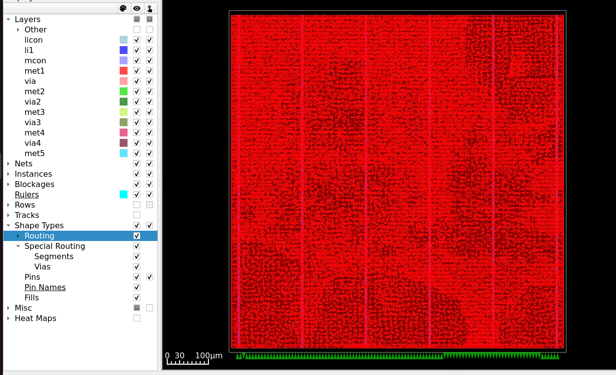
Fig. 9 Post-CTS layout of aes_wb_wrapper — standard cells placed, Wishbone pins constrained to the South edge.
Tracing the Clock Tree
Step 1 — Open the Clock Tree Viewer: From the top menu bar, select Windows → Clock Tree Viewer.
Step 2 — Render the tree:
In the Clock Tree Viewer panel on the right-hand side, click Update in the
top-right corner to render the full hierarchical H-Tree for aes_wb_wrapper.
Tip
For a cleaner view, disable all metal layers in Display Control → Layers on the left sidebar. This removes routing clutter, leaving only the clock tree structure visible in the main canvas.
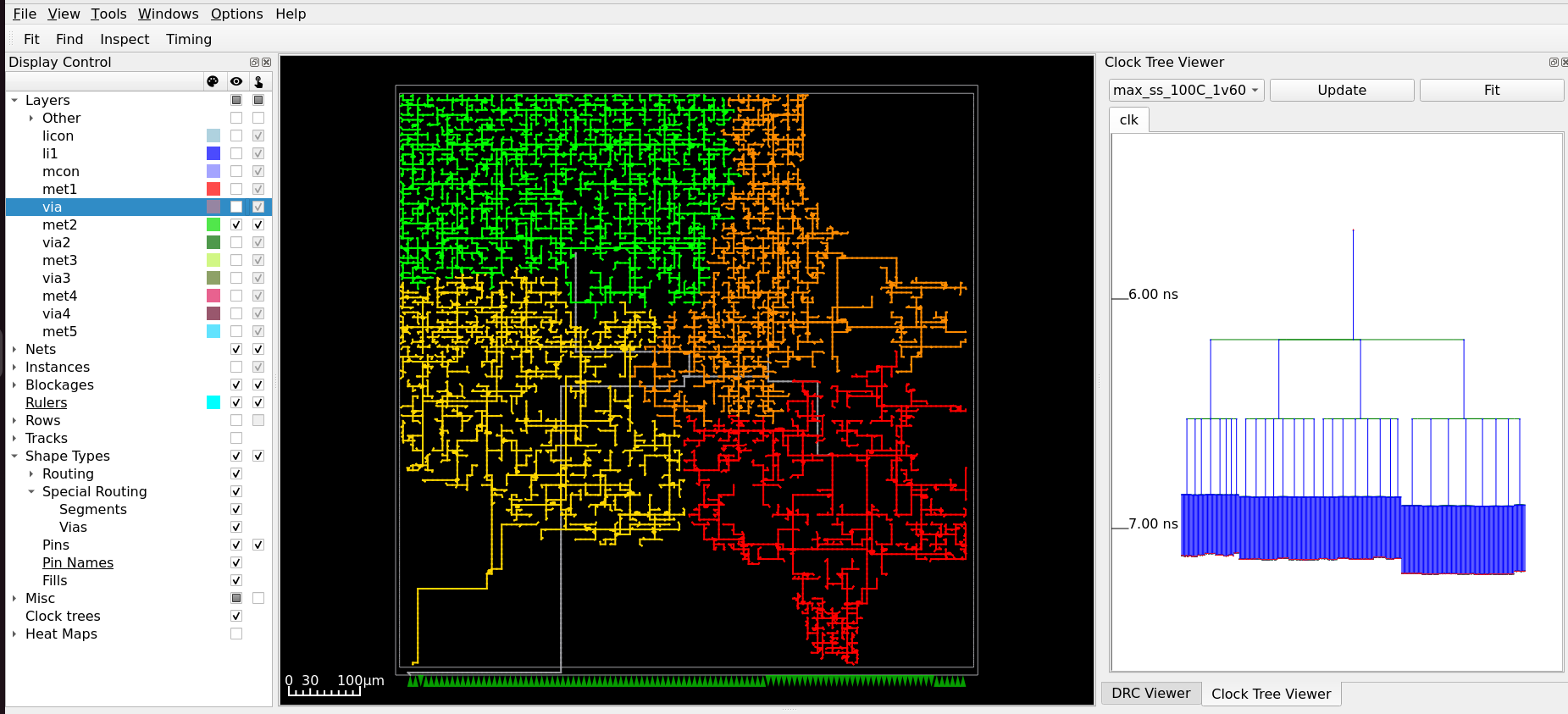
Fig. 10 Clock Tree Viewer — synthesised H-Tree topology for aes_wb_wrapper, with metal layers hidden.
Using Heat Maps
OpenROAD provides heat map overlays for analysing the spatial distribution of placement density and power dissipation.
Placement Density — From the menu bar, select Tools → Heat Maps → Placement Density.
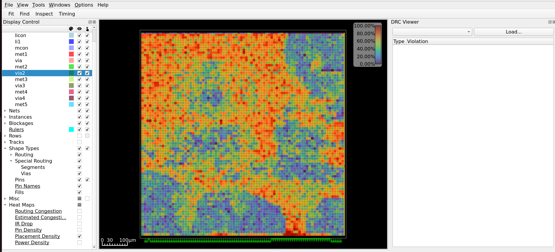
Fig. 11 Placement Density heat map — warmer colours indicate higher standard cell density.
Power Density — From Display Control, expand Heat Maps and select Power Density.
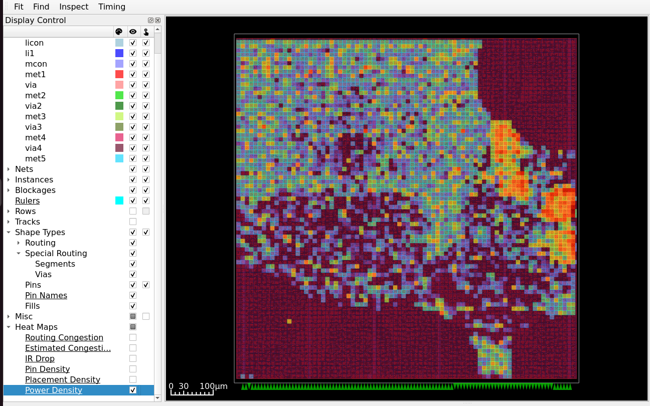
Fig. 12 Power Density heat map — highlights regions of high switching activity in the AES datapath.
Inspecting Timing Paths
From the menu bar, select Windows → Timing Report.
In the Timing Report panel:
Select the Hold tab to check paths where data arrives too quickly.
Click Paths → Update and enter an integer number of paths to display.
Positive slack confirms the design is safe and meets the hold constraint.
Fig. 13 Timing Report panel — ranked list of Hold paths after Post-CTS repair.
The tool inserts delay gates (dlygate) and clock-delay buffers (clkdlybuf)
as “speed bumps” to slow data propagation and fix Hold violations. Select any path to
view the full Data Path Details showing every gate the signal passes through,
with pin name, cumulative time, delay, slew, and load values.
Fig. 14 Data Path Details — pin-level breakdown of the worst Hold path after CTS repair.
Inspecting Intermediate Flow Steps
Any intermediate step can be loaded in the GUI using its state_out.json and
--with-initial-state. To inspect the design after Global Placement — before
Detailed Placement resolves cell overlaps:
[nix-shell:~]$ librelane \
    ~/Silicon-Sprint-AUC/openlane/aes_wb_wrapper/config.json \
    --flow openinopenroad \
    --with-initial-state \
    ~/Silicon-Sprint-AUC/openlane/aes_wb_wrapper/runs/classic_flow/24-openroad-globalplacementskipio/state_out.json
Note
At the Global Placement stage, cell positions are optimised for wire length but overlaps are not yet resolved — this is expected. Detailed Placement (the following step) legalises the layout by aligning cells to site rows and eliminating all overlaps. Comparing the two states side by side is one of the most instructive visualisations in the entire ASIC flow.
Fig. 15 Global Placement state — cell overlaps visible before Detailed Placement legalisation.
Timing and Design Rule Reports (Post-CTS)
After OpenROAD.STAMidPNR-2 completes, analyse the reports in
runs/classic_flow/38-openroad-stamidpnr-2/ to verify design health before
routing begins.
Design Rule Violations (DRVs)
Location: 38-openroad-stamidpnr-2/max_ss_100C_1v60/checks.rpt
max slew violation count 121
max fanout violation count 2
max cap violation count 0
Note
All violations are evaluated at the max_ss_100C_1v60 corner — the worst-case
combination of slow transistors, high temperature, and low voltage. The 121 remaining
Max Slew violations are expected at this mid-flow stage; the post-GRT repair pass in
Module 3 and ECO buffers in Module 4 resolve them before signoff.
Slack Analysis
Metric |
Report File |
Value (ns) |
|---|---|---|
Worst Setup Slack |
|
+3.58 |
Worst Hold Slack |
|
+0.589 |
Note
The Hold WNS of +0.589 ns is measured at the Slow-Slow corner. At the
Fast-Fast corner (max_ff_n40C_1v95) — where cells switch faster and hold paths
become harder to meet — this margin decreases significantly, often approaching
+0.1–0.2 ns at signoff. The post-CTS hold repair pass tightens this further.
Clock Skew Analysis
Location: 38-openroad-stamidpnr-2/max_ss_100C_1v60/skew.max.rpt
Clock skew is the difference in arrival time of the clock edge at two different flip-flop clock pins, caused by imbalances in the clock tree buffers or their physical placement. In setup analysis, the worst case is when the launch clock arrives later and the capture clock arrives earlier — consuming setup margin.
===========================================================================
Clock Skew (Setup)
============================================================================
Writing metric clock__skew__worst_setup__corner:max_ss_100C_1v60: 0.40678306319200896
======================= max_ss_100C_1v60 Corner ===================================

Clock clk
7.624432 source latency _42992_/CLK ^
-5.961826 target latency _43086_/CLK ^
0.120000 clock uncertainty
-1.375823 CRPR
--------------
0.406783 setup skew
Calculating Skew — A Worked Example
The numbers in the skew report can be verified by tracing a real timing path. The following report shows the complete launch and capture clock paths for a register-to-register setup check.
Timing Path Report — Setup Analysis
Startpoint: _42738_ (rising edge-triggered flip-flop clocked by clk)
Endpoint:   _44942_ (rising edge-triggered flip-flop clocked by clk)
Path Group: clk
Path Type:  max

Fanout         Cap        Slew       Delay        Time   Description
---------------------------------------------------------------------------------------------
                                  0.000000    0.000000   clock clk (rise edge)
                                  5.700000    5.700000   clock source latency
     1    0.072162    0.610000    0.000000    5.700000 ^ wb_clk_i (in)
                      0.629538    0.010453    5.710453 ^ clkbuf_0_wb_clk_i/A (sky130_fd_sc_hd__clkbuf_16)
     4    0.079672    0.152720    0.567149    6.277601 ^ clkbuf_0_wb_clk_i/X (sky130_fd_sc_hd__clkbuf_16)
                      0.152780    0.003065    6.280666 ^ clkbuf_2_1_0_wb_clk_i/A (sky130_fd_sc_hd__clkbuf_8)
     8    0.135697    0.363312    0.525664    6.806330 ^ clkbuf_2_1_0_wb_clk_i/X (sky130_fd_sc_hd__clkbuf_8)
                      0.363338    0.003589    6.809919 ^ clkbuf_5_9__f_wb_clk_i/A (sky130_fd_sc_hd__clkbuf_16)
     9    0.070258    0.136613    0.440059    7.249978 ^ clkbuf_5_9__f_wb_clk_i/X (sky130_fd_sc_hd__clkbuf_16)
                      0.136615    0.000813    7.250791 ^ clkbuf_leaf_302_wb_clk_i/A (sky130_fd_sc_hd__clkbuf_8)
    10    0.026497    0.098846    0.300852    7.551643 ^ clkbuf_leaf_302_wb_clk_i/X (sky130_fd_sc_hd__clkbuf_8)
                      0.098846    0.000025    7.551668 ^ _42738_/CLK (sky130_fd_sc_hd__dfrtp_2)
     1    0.002784    0.071394    0.733986    8.285654 ^ _42738_/Q (sky130_fd_sc_hd__dfrtp_2)
                      0.071394    0.000009    8.285663 ^ fanout1794/A (sky130_fd_sc_hd__clkdlybuf4s25_1)
     5    0.015919    0.275160    0.652499    8.938162 ^ fanout1794/X (sky130_fd_sc_hd__clkdlybuf4s25_1)
                      0.275160    0.000074    8.938235 ^ wire1795/A (sky130_fd_sc_hd__clkbuf_4)
     5    0.036924    0.191644    0.460672    9.398907 ^ wire1795/X (sky130_fd_sc_hd__clkbuf_4)
...
                      0.042380    0.000007   24.621771 v _44942_/D (sky130_fd_sc_hd__dfrtp_2)
                                             24.621771   data arrival time

                                 25.000000   25.000000   clock clk (rise edge)
                                  4.400000   29.400000   clock source latency
     1    0.072162    0.610000    0.000000   29.400000 ^ wb_clk_i (in)
                      0.629538    0.009084   29.409084 ^ clkbuf_0_wb_clk_i/A (sky130_fd_sc_hd__clkbuf_16)
     4    0.079672    0.152720    0.492943   29.902027 ^ clkbuf_0_wb_clk_i/X (sky130_fd_sc_hd__clkbuf_16)
                      0.152806    0.003087   29.905113 ^ clkbuf_2_2_0_wb_clk_i/A (sky130_fd_sc_hd__clkbuf_8)
     8    0.124382    0.337152    0.438025   30.343138 ^ clkbuf_2_2_0_wb_clk_i/X (sky130_fd_sc_hd__clkbuf_8)
                      0.337194    0.003560   30.346699 ^ clkbuf_5_20__f_wb_clk_i/A (sky130_fd_sc_hd__clkbuf_16)
    16    0.107587    0.187924    0.410296   30.756994 ^ clkbuf_5_20__f_wb_clk_i/X (sky130_fd_sc_hd__clkbuf_16)
                      0.187930    0.001226   30.758221 ^ clkbuf_leaf_67_wb_clk_i/A (sky130_fd_sc_hd__clkbuf_8)
    11    0.027302    0.100911    0.285311   31.043531 ^ clkbuf_leaf_67_wb_clk_i/X (sky130_fd_sc_hd__clkbuf_8)
                      0.100911    0.000046   31.043577 ^ _44942_/CLK (sky130_fd_sc_hd__dfrtp_2)
                                 -0.120000   30.923578   clock uncertainty
                                  1.375574   32.299152   clock reconvergence pessimism
                                 -0.256838   32.042316   library setup time
                                             32.042316   data required time
---------------------------------------------------------------------------------------------
                                             32.042316   data required time
                                            -24.621771   data arrival time
---------------------------------------------------------------------------------------------
                                              7.420546   slack (MET)
Step 1 — Launch clock latency (time from clock source to _42738_/CLK):
Step 2 — Capture clock latency (absolute time to _44942_/CLK, minus one clock period to find the insertion delay):
Step 3 — Adjustments applied to the capture path:
Adjustment |
Value (ns) |
Direction |
Effect on Setup Analysis |
|---|---|---|---|
Clock uncertainty |
−0.120 |
Subtracted from capture |
Models worst-case early arrival of capture edge — makes setup harder to meet |
CRPR |
+1.375574 |
Added to capture |
Removes artificial pessimism from shared clock path buffers (see below) |
Step 4 — Skew calculation:
The negative result confirms that the launch path (_42738_) is slower than the
capture path (_44942_). Data must therefore travel a longer absolute time to reach
the endpoint, which is the adverse skew scenario for setup timing.
Clock Reconvergence Pessimism Removal (CRPR)
The launch and capture clock paths both originate from the same root buffers —
clkbuf_0_wb_clk_i and clkbuf_2_x_0_wb_clk_i are visible in both sections of
the timing report. In worst-case analysis, STA independently assumes the
shared portion of the launch path is slow and the shared portion of the capture
path is fast simultaneously — which is physically impossible. A single buffer
cannot be both fast and slow at the same time.
CRPR corrects this by adding back the maximum variation that was double-counted on the shared path segment, making the analysis physically realistic.
Fig. 16 Clock Reconvergence Pessimism — shared root buffers cannot simultaneously be slow for the launch path and fast for the capture path. CRPR credits back the over-counted variation, improving setup slack.
Non-Default Routing Rules (NDR) for the Clock
OpenROAD can route clock nets using Non-Default Rules (NDR) — wider metal tracks and increased spacing compared to standard signal wires. Wider, more widely spaced clock routes are less susceptible to crosstalk coupling from adjacent signal nets and to electromigration effects under high switching currents.
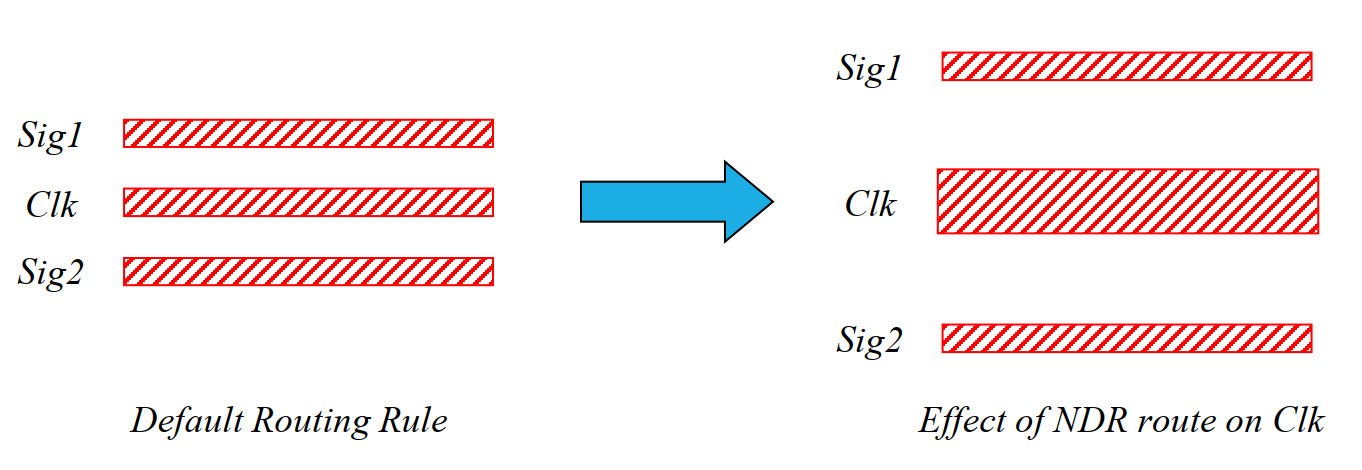
Fig. 17 Non-Default Routing Rule — clock net routed with 2× width and 2× spacing compared to a signal wire, reducing capacitive crosstalk coupling.
NDRs are defined in config.json. The example below defines a rule named clkndr
with doubled width and spacing on Metal 2–4, and applies it to the wb_clk_i net:
"NON_DEFAULT_RULES": {
    "clkndr": {
        "width":   "met2 0.28 met3 0.6 met4 0.6",
        "spacing": "met2 0.28 met3 0.6 met4 0.6",
        "via": "None"
    }
},
"CTS_APPLY_NDR": "full",
"DRT_ASSIGN_NDR": {
    "wb_clk_i": "clkndr"
}
Note
This example is for explanation only — it is not used in the workshop configuration.
The default value of CTS_APPLY_NDR is “half”, which applies the 2X spacing NDR to clock nets except for the leaf-level nets This strategy protects the main branches of the clock tree from crosstalk while preventing routing congestion near the dense logic where leaf wires reside. The “full” option extends the rule to the entire tree, including the leaves
The default metal dimensions for SkyWater 130nm are found in the technology LEF:
$ cat ~/.ciel/ciel/sky130/versions/8afc8346a57fe1ab7934ba5a6056ea8b43078e71/sky130B/\
libs.ref/sky130_fd_sc_hd/techlef/sky130_fd_sc_hd__nom.tlef
The Metal 2 entry (the default vertical clock routing layer) shows:
LAYER met2
  TYPE ROUTING ;
  DIRECTION VERTICAL ;
  PITCH 0.46 ;
  WIDTH 0.14 ;
  SPACINGTABLE
     PARALLELRUNLENGTH 0
     WIDTH 0   0.14
     WIDTH 3   0.28 ;
The NDR in the example above doubles both the width (0.14 → 0.28 µm) and the
minimum spacing (0.14 → 0.28 µm) on Metal 2, providing a 2× crosstalk guard-band
for the clock net at the cost of consuming twice as many routing tracks on that layer.
- I/O
Input/Output. The physical pins on a macro or chip boundary through which signals enter and leave the design.
- DRC
Design Rule Check. Verification that the physical layout conforms to the foundry’s manufacturing constraints.
- STA
Static Timing Analysis. Timing verification performed by exhaustively checking all signal paths against declared constraints without requiring simulation vectors.
- CTS
Clock Tree Synthesis. The physical design step that constructs a balanced clock distribution network to minimise clock skew across all sequential elements.
- SDC
Synopsys Design Constraints. A Tcl-based format specifying timing and clocking constraints for implementation and static timing analysis.
- PnR
Place and Route. The physical design stage encompassing standard cell placement and signal wire routing.
- WNS
Worst Negative Slack. The largest magnitude of negative slack across all failing timing paths.
- TNS
Total Negative Slack. The arithmetic sum of all negative slack values across every failing timing path.
- flip-flop
A bistable sequential logic element that stores one bit of state, clocked by the design’s primary clock signal.
- clock skew
The difference in clock arrival time between two sequential elements. Excessive skew causes Hold violations on short paths and degrades Setup margin on long paths.
- PPA
Power, Performance, Area. The three primary optimisation axes in VLSI design.