Module 4: Physical Signoff
Prerequisites
Before proceeding, ensure your Module 3 routing run (classic_flow) has completed
successfully through step 52-checker-wirelength. The signoff flow resumes from
this checkpoint using --with-initial-state.
Table of Contents
1. Signoff Flow Overview
The signoff stage transforms a fully routed design into a verified, manufacturable chip. It is divided into two phases that are executed separately in this module:
Signoff Prep — electrical and timing verification (Fill, RCX, STA, IR Drop).
Physical Signoff — geometric and connectivity verification (GDS, DRC, LVS).
Separating the two phases allows us to analyse the timing reports, resolve any remaining violations using an ECO (Engineering Change Order), and only then commit to the final physical checks.
Phase |
Step Description |
Step ID |
|---|---|---|
Signoff Prep |
Fill Cell Insertion |
|
Cell Frequency Tables |
|
|
Parasitic Extraction |
|
|
Post-PnR Static Timing Analysis |
|
|
IR Drop Reporting |
|
|
Physical Signoff |
GDSII Stream Out (Magic) |
|
GDSII Stream Out (KLayout) |
|
|
KLayout Render |
|
|
Write Macro LEF |
|
|
Check Design Antenna Properties |
|
|
XOR GDS Comparison |
|
|
XOR Comparison Check |
|
|
Physical DRC (Magic) |
|
|
Physical DRC (KLayout) |
|
|
Magic DRC Check |
|
|
KLayout DRC Check |
|
|
SPICE Netlist Extraction |
|
|
Illegal Overlap Check |
|
|
Layout vs. Schematic (LVS) |
|
|
LVS Comparison Check |
|
|
Formal Equivalence Check |
|
|
Setup / Hold Violations Check |
|
|
Max Slew / Cap Violations Check |
|
|
Final Manufacturability Report |
|
2. Signoff Prep
2.1 Fill Cell Insertion (OpenROAD.FillInsertion)
After Detailed Routing completes, the standard cell rows contain physical gaps between
functional cells. The FillInsertion step closes every gap by inserting filler cells
and decap cells across the entire layout.
Note
This step marks a critical design boundary. After fill insertion, the design is functionally frozen — all logic, buffers, clock cells, and antenna diodes are locked in place. Filler cells occupy the remaining silicon area, completing the physical fabric of the chip.
What Filler Cells Do
Role |
Why It Matters |
|---|---|
N-well / P-well Continuity |
Standard cells require continuous substrate wells across every row. Gaps break these wells. Filler cells bridge them, ensuring a single uninterrupted implant mask layer. |
Power Rail Continuity (VDD/VSS) |
Horizontal Metal 1 power rails must be electrically connected across the entire row. Without fillers these rails float in empty spaces, creating localised IR drop. Fillers act as a conductor bridge for the power grid. |
Manufacturing Yield |
Empty spaces create density gradients during CMP, leading to surface defects. Filling all gaps ensures uniform density and maximises the ratio of functional dies per wafer. |
For the aes_wb_wrapper, fill insertion produces the following final cell population:
Cell type report:                       Count       Area
  Fill cell                             97238  331153.85
  Tap cell                               9176   11481.01
  Antenna cell                            959    2399.80
  Buffer                                 4273   19533.73
  Clock buffer                            549    7302.00
  Timing Repair Buffer                   3070   26057.49
  Inverter                               3113   11684.96
  Clock inverter                           90    1127.33
  Sequential cell                        2995   78696.73
  Multi-Input combinational cell        13795  151730.52
  Total                                135258  641167.43
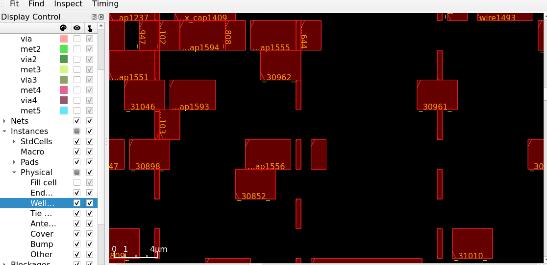
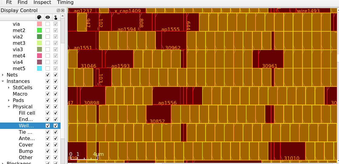
The figures below show the layout before and after fill insertion:
2.2 Parasitic Extraction (OpenROAD.RCX)
With the layout physically complete, the OpenRCX engine converts routed geometry into an electrical model. Every wire has real resistance (from its length and cross-section) and real capacitance (from its proximity to adjacent wires and the substrate). Parasitic extraction captures these values so the downstream STA uses actual physical delays instead of statistical estimates.
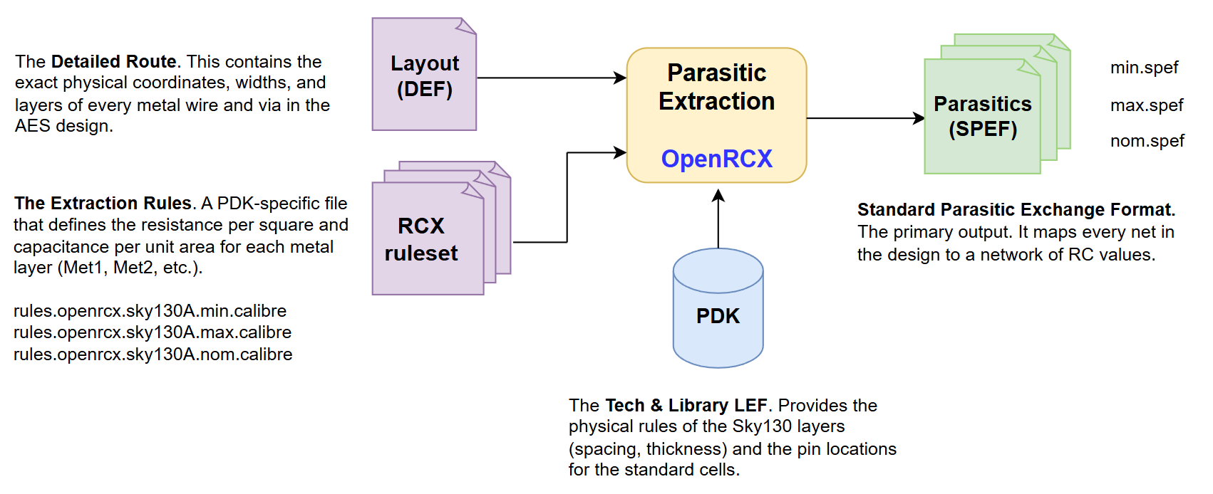
Fig. 25 OpenRCX inputs and outputs — the extraction bridge between physical geometry and electrical models.
The Extraction Process
RC Segment Generation — Each physical wire is broken into smaller electrical
segments. Resistance is calculated per segment from layer, width, and length.
Via resistance is added at every layer transition. For aes_wb_wrapper this yields
161,601 RC segments across 27,332 nets.
Capacitance Calculation:
Coupling capacitance — electrical interaction between parallel wires on the same layer. The primary mechanism for crosstalk on critical timing paths.
Ground capacitance — capacitance between a wire and the substrate or ground planes.
Filtering — Coupling values below 0.1 fF are merged into ground capacitance, simplifying the SPEF without meaningful accuracy loss.
Output — Three Corner SPEF Files
runs/classic_flow/55-openroad-rcx/
    ├── max/   aes_wb_wrapper.max.spef  ← Worst-case RC — used for Setup analysis
    ├── nom/   aes_wb_wrapper.nom.spef  ← Nominal RC
    └── min/   aes_wb_wrapper.min.spef  ← Best-case RC — used for Hold analysis
The SPEF (Standard Parasitic Exchange Format) file maps the resistance and capacitance of every net. It feeds directly into the Post-PnR STA engine, enabling the first silicon-accurate timing analysis.
2.3 Post-PnR Static Timing Analysis (OpenROAD.STAPostPNR)
Fig. 26 Post-PnR STA flow — SPEF parasitics enable physically accurate timing analysis for the first time.
This is the most authoritative timing check in the entire flow. The OpenSTA engine analyses the completed physical netlist annotated with exact RC parasitics from RCX.
Analysis Stage |
Parasitic Source |
Accuracy |
|---|---|---|
Pre-PnR STA (Module 1) |
Statistical wire-load models |
Low — estimates only |
Mid-PnR STA (Modules 2–3) |
Global routing RC estimates |
Medium — approximate |
Post-PnR STA (this step) |
RCX SPEF — actual wire geometry |
High — silicon-accurate |
Multi-Corner Analysis
The analysis covers 9 PVT corners — three process splits (max / nom / min) for each of three temperature-voltage combinations:
max_ss_100C_1v60    nom_ss_100C_1v60    min_ss_100C_1v60
max_tt_025C_1v80    nom_tt_025C_1v80    min_tt_025C_1v80
max_ff_n40C_1v95    nom_ff_n40C_1v95    min_ff_n40C_1v95
Note
Earlier STA stages analyse only 3 corners. Post-PnR STA expands to 9 corners, providing complete coverage of the PVT space for final signoff.
Each corner produces a dedicated directory of reports:
runs/classic_flow/56-openroad-stapostpnr/
└── max_ff_n40C_1v95/
    ├── aes_wb_wrapper__max_ff_n40C_1v95.lib   ← Liberty timing model
    ├── aes_wb_wrapper__max_ff_n40C_1v95.sdf   ← Standard Delay Format
    ├── max.rpt / min.rpt                       ← Setup / Hold constrained paths
    ├── wns.max.rpt / wns.min.rpt              ← Worst Negative Setup / Hold Slack
    ├── tns.max.rpt / tns.min.rpt              ← Total Negative Slack
    ├── ws.max.rpt / ws.min.rpt                ← Worst Setup / Hold Slack
    ├── skew.max.rpt / skew.min.rpt            ← Clock skew
    ├── power.rpt                               ← Corner power breakdown
    ├── checks.rpt                              ← Max Cap, Slew, Fanout, unconstrained
    ├── violator_list.rpt                       ← All failing endpoints
    ├── clock.rpt / unpropagated.rpt
    └── sta.log                                 ← Full raw STA engine output
2.4 IR Drop Analysis (OpenROAD.IRDropReport)
This step performs a static IR drop analysis on the completed PDN. Every wire in the power and ground network has resistance, causing a voltage drop as current flows from the supply pads to the standard cells.
The tool evaluates both networks separately:
VPWR: Voltage decrease from supply to cells (classical IR drop). Excessive drop slows logic and degrades setup margin.VGND: Voltage rise on the ground return path (ground bounce). This reduces the effective noise margin of every standard cell in the affected region.
Analysis is performed on max_ss_100C_1v60 — the worst-case combination of
maximum wire resistance and highest current demand.
Report location:
runs/classic_flow/57-openroad-irdropreport/irdrop.rpt
3. Running the Signoff Prep Flow
This run executes all Signoff Prep steps and stops after IR Drop Analysis, allowing us to review the electrical results before committing to the physical signoff steps.
Ensure you are inside the Nix shell:
$ nix-shell --pure ~/librelane/shell.nix
Then execute:
[nix-shell:~]$ librelane \
    ~/Silicon-Sprint-AUC/openlane/aes_wb_wrapper/config.json \
    --run-tag classic_flow \
    --from OpenROAD.FillInsertion \
    --to OpenROAD.IRDropReport \
    --with-initial-state \
    ~/Silicon-Sprint-AUC/openlane/aes_wb_wrapper/runs/classic_flow/52-checker-wirelength/state_out.json
The run will execute through the following steps:
runs/classic_flow/
    ⋮
    ├── 53-openroad-fillinsertion/
    ├── 54-odb-cellfrequencytables/
    ├── 55-openroad-rcx/
    │   ├── max/   aes_wb_wrapper.max.spef
    │   ├── nom/   aes_wb_wrapper.nom.spef
    │   └── min/   aes_wb_wrapper.min.spef
    ├── 56-openroad-stapostpnr/     ← 9-corner STA with SPEF parasitics
    └── 57-openroad-irdropreport/   ← PDN voltage drop analysis
4. Signoff Prep Results Analysis
4.1 Post-PnR STA Report
Location: runs/classic_flow/56-openroad-stapostpnr/summary.rpt
┏━━━━━━━━━━━━━━━━━━━━━━┳━━━━━━━━━━┳━━━━━━━━━━┳━━━━━━━━━━┳━━━━━━━━━━┳━━━━━━━━━━━┳━━━━━━━━━━┳━━━━━━━━━━━┳━━━━━━━━━━┳━━━━━━━━━━━┳━━━━━━━━━━┳━━━━━━━━━━━┳━━━━━━━━━━┓
┃                      ┃ Hold     ┃ Reg to   ┃          ┃          ┃ of which  ┃ Setup    ┃           ┃          ┃           ┃ of which ┃           ┃          ┃
┃                      ┃ Worst    ┃ Reg      ┃          ┃ Hold Vio ┃ reg to    ┃ Worst    ┃ Reg to    ┃ Setup    ┃ Setup Vio ┃ reg to   ┃ Max Cap   ┃ Max Slew ┃
┃ Corner/Group         ┃ Slack    ┃ Paths    ┃ Hold TNS ┃ Count    ┃ reg       ┃ Slack    ┃ Reg Paths ┃ TNS      ┃ Count     ┃ reg      ┃ Violatio… ┃ Violati… ┃
┡━━━━━━━━━━━━━━━━━━━━━━╇━━━━━━━━━━╇━━━━━━━━━━╇━━━━━━━━━━╇━━━━━━━━━━╇━━━━━━━━━━━╇━━━━━━━━━━╇━━━━━━━━━━━╇━━━━━━━━━━╇━━━━━━━━━━━╇━━━━━━━━━━╇━━━━━━━━━━━╇━━━━━━━━━━┩
│ Overall              │ 0.0976   │ 0.0976   │ 0.0000   │ 0        │ 0         │ 0.9654   │ 0.9654    │ 0.0000   │ 0         │ 0        │ 4         │ 15       │
│ nom_tt_025C_1v80     │ 0.2467   │ 0.2467   │ 0.0000   │ 0        │ 0         │ 8.3476   │ 12.8800   │ 0.0000   │ 0         │ 0        │ 0         │ 0        │
│ nom_ss_100C_1v60     │ 0.6349   │ 0.6349   │ 0.0000   │ 0        │ 0         │ 1.4718   │ 1.4718    │ 0.0000   │ 0         │ 0        │ 2         │ 4        │
│ nom_ff_n40C_1v95     │ 0.1129   │ 0.1129   │ 0.0000   │ 0        │ 0         │ 9.3891   │ 17.1946   │ 0.0000   │ 0         │ 0        │ 0         │ 0        │
│ min_tt_025C_1v80     │ 0.2603   │ 0.2603   │ 0.0000   │ 0        │ 0         │ 8.4851   │ 13.1686   │ 0.0000   │ 0         │ 0        │ 0         │ 0        │
│ min_ss_100C_1v60     │ 0.6385   │ 0.6385   │ 0.0000   │ 0        │ 0         │ 1.9956   │ 1.9956    │ 0.0000   │ 0         │ 0        │ 2         │ 4        │
│ min_ff_n40C_1v95     │ 0.1233   │ 0.1233   │ 0.0000   │ 0        │ 0         │ 9.4797   │ 17.4495   │ 0.0000   │ 0         │ 0        │ 0         │ 0        │
│ max_tt_025C_1v80     │ 0.2244   │ 0.2244   │ 0.0000   │ 0        │ 0         │ 8.2340   │ 12.5911   │ 0.0000   │ 0         │ 0        │ 0         │ 0        │
│ max_ss_100C_1v60     │ 0.6040   │ 0.6040   │ 0.0000   │ 0        │ 0         │ 0.9654   │ 0.9654    │ 0.0000   │ 0         │ 0        │ 4         │ 15       │
│ max_ff_n40C_1v95     │ 0.0976   │ 0.0976   │ 0.0000   │ 0        │ 0         │ 9.3101   │ 16.9422   │ 0.0000   │ 0         │ 0        │ 0         │ 0        │
└──────────────────────┴──────────┴──────────┴──────────┴──────────┴───────────┴──────────┴───────────┴──────────┴───────────┴──────────┴───────────┴──────────┘
Interpreting the Post-PnR STA Results
Hold violations: fully resolved. All 9 corners show positive Hold WNS (≥ +0.1086 ns). The CTS and post-CTS repair passes from Module 2 closed every hold path.
Setup timing: clean. Zero Setup violations across all 9 corners. The positive Setup WNS values confirm the design meets the 40 MHz target under all conditions.
Max Slew / Max Cap: require attention. The max_ss_100C_1v60 corner shows
14 Max Slew and 5 Max Cap violations. These must be resolved before physical
signoff. See Section 5.
Hold Slack margin. The worst Hold WNS is only +0.0976 ns in the
max_ff_n40C_1v95 corner. While technically passing, this narrow margin may become
a Hold violation when the macro is integrated into the Caravel top level, as the
wrapper’s routing adds additional clock path delays. The ECO step also addresses this.
4.2 Power Report
Location: runs/classic_flow/56-openroad-stapostpnr/max_ff_n40C_1v95/power.rpt
Worst-case power occurs at max_ff_n40C_1v95 — fast transistors at low temperature
and high voltage switching at maximum rate:
======================= max_ff_n40C_1v95 Corner ===================================
Group                    Internal    Switching      Leakage        Total
                            Power        Power        Power        Power (Watts)
------------------------------------------------------------------------
Sequential           5.653847e-03 6.869405e-05 6.859135e-08 5.722610e-03  30.8%
Combinational        2.391679e-03 5.279127e-03 2.687200e-07 7.671075e-03  41.3%
Clock                2.375699e-03 2.799051e-03 3.273007e-07 5.175077e-03  27.9%
Macro                0.000000e+00 0.000000e+00 0.000000e+00 0.000000e+00   0.0%
Pad                  0.000000e+00 0.000000e+00 0.000000e+00 0.000000e+00   0.0%
------------------------------------------------------------------------
Total                1.042120e-02 8.146887e-03 6.646642e-07 1.856875e-02 100.0%
                            56.1%        43.9%         0.0%
Note
Combinational logic (41.3%) dominates, driven by switching activity in the AES datapath — XOR, shift, and S-box substitution operations. The clock network (27.9%) reflects distributing the clock to ~3,000 flip-flops via a balanced H-Tree. Total power of ~18.6 mW is well within the Caravel User Project power budget.
4.3 IR Drop Report
Location: runs/classic_flow/57-openroad-irdropreport/irdrop.rpt
########## IR report #################
Net              : VPWR
Corner           : max_ss_100C_1v60
Supply voltage   : 1.60e+00 V
Average IR drop  : 9.82e-05 V
Worstcase IR drop: 8.13e-04 V
Percentage drop  : 0.05 %
######################################

########## IR report #################
Net              : VGND
Corner           : max_ss_100C_1v60
Supply voltage   : 0.00e+00 V
Average IR drop  : 9.74e-05 V
Worstcase IR drop: 7.47e-04 V
Percentage drop  : 0.05 %
######################################
IR Drop — Excellent PDN Health
Worst-case IR drop of 0.05% on both VPWR and VGND — well within the industry
signoff requirement of < 2–5%. This confirms that the PDN design choices from
Module 1 (PDN_MULTILAYER: false, Metal 4 vertical straps) provide stable power
delivery under worst-case conditions. No hotspots or under-powered regions exist
in the core.
5. Resolving Max Slew and Max Cap
The STA report reveals two categories of issues that must be addressed before physical signoff can proceed:
Max Slew (20) and Max Cap (5) violations in the
max_ss_100C_1v60corner.Narrow Hold WNS (+0.11 ns) in the
max_ff_n40C_1v95corner — technically passing, but at risk of becoming a Hold violation when integrated into Caravel due to additional clock path delays introduced by the top-level wrapper routing.
5.1 Diagnosing the Violations
Open the checks.rpt for the worst-case corner:
runs/classic_flow/56-openroad-stapostpnr/max_ss_100C_1v60/checks.rpt
The report shows the specific violating pins and the magnitude of each violation:
Max Slew Violations:
max slew

Pin                                        Limit        Slew       Slack
------------------------------------------------------------------------
wire640/A                               1.500000    2.107202   -0.607202 (VIOLATED)
_32342_/Y                               1.500000    2.107156   -0.607156 (VIOLATED)
wire815/A                               1.500000    2.055321   -0.555321 (VIOLATED)
_31400_/Y                               1.500000    2.055185   -0.555185 (VIOLATED)
fanout1989/A                            1.500000    1.541561   -0.041561 (VIOLATED)
_21421_/S1                              1.500000    1.541495   -0.041495 (VIOLATED)
_23566_/S1                              1.500000    1.541461   -0.041461 (VIOLATED)
_23576_/S1                              1.500000    1.541394   -0.041394 (VIOLATED)
_31836_/A1                              1.500000    1.541291   -0.041291 (VIOLATED)
_33183_/A1                              1.500000    1.541274   -0.041274 (VIOLATED)
_30878_/A                               1.500000    1.541205   -0.041205 (VIOLATED)
fanout1986/A                            1.500000    1.541202   -0.041202 (VIOLATED)
fanout1992/X                            1.500000    1.541190   -0.041190 (VIOLATED)
_31884_/X                               1.494952    1.507921   -0.012969 (VIOLATED)
_31885_/B                               1.500000    1.508484   -0.008484 (VIOLATED)
Max Cap Violations:
max capacitance

Pin                                        Limit         Cap       Slack
------------------------------------------------------------------------
_32342_/Y                               0.051280    0.076849   -0.025569 (VIOLATED)
_31400_/Y                               0.051280    0.074715   -0.023435 (VIOLATED)
fanout1992/X                            0.081492    0.083940   -0.002448 (VIOLATED)
_31884_/X                               0.108042    0.109550   -0.001508 (VIOLATED)
Note
Notice that _32342_/Y, _31400_/Y, fanout1992/X, and _31884_/X appear in both
the Max Slew and Max Cap violation lists. This is the expected coupling: an overloaded
output capacitance on the driver directly causes a slow transition on every input it
drives. Fixing the cap violation will simultaneously resolve the corresponding slew
violation on the same net.
Worst Hold Slack:
In the Post-PnR stage, we analyze the Fast Corner (Minimum Delay) to ensure data does not move through the logic too quickly, which would cause a race condition.
To find the most critical hold path, we inspect the timing report generated for the best-case silicon conditions:
File:
runs/classic_flow/56-openroad-stapostpnr/max_ff_n40C_1v95/min.rptandruns/classic_flow/56-openroad-stapostpnr/min_ff_n40C_1v95/min.rptAnalysis: We locate the first path in the report, which shows the worst slack of 0.11.
Target Pin: By tracing the Arrival Path, we identify the output of the launch Flip-Flop:
_45051_/Qformax_ff_n40C_1v95/min.rptand 42587/Q formin_ff_n40C_1v95.
To increase the hold margin, we must intentionally add delay to this specific path. By inserting 2 buffers immediately after the launch pin, we ensure the data stays stable long enough to meet the hold requirement of the capturing register.
5.2 ECO Buffer Insertion — Side Load Isolation
The solution is to insert strong driver buffers (sky130_fd_sc_hd__buf_4) at the
output of each overloaded gate — an Engineering Change Order (ECO) performed
post-routing. This technique is called Side Load Isolation:
Fig. 27 Side Load Isolation — a buf_4 is inserted after the overloaded driver, absorbing the heavy capacitive load so the original gate only drives the small buffer input.
Why target the driver output pin?
By inserting a buffer immediately after _33732_/Y (for example), the original gate
only needs to charge the tiny input capacitance of the buf_4. The buf_4 then
handles the heavy capacitive load of the long downstream wire (wire709). The original
gate’s slew improves, the cap violation clears, and wire709 receives a strongly driven
signal.
Step 1 — Add the ECO Flow to config.json
LibreLane performs ECO buffer insertion as a substitution step that is injected
just before the final Detailed Routing re-run. Add the meta flow substitution block
to your config.json:
{
   "DESIGN_NAME": "aes_wb_wrapper",
    "PDN_MULTILAYER": false,
    "CLOCK_PORT": "wb_clk_i",
    "CLOCK_PERIOD": 25,
    "VERILOG_FILES": [
        "dir::../../../secworks_aes/src/rtl/*.v",
        "dir::../../verilog/rtl/aes_wb_wrapper.v"
    ],
    "FP_CORE_UTIL": 40,
    "RT_MAX_LAYER": "met4",
    "SYNTH_STRATEGY": "DELAY 4",
    "DEFAULT_CORNER": "max_ss_100C_1v60",
    "RUN_POST_GRT_DESIGN_REPAIR": true,
    "PNR_SDC_FILE": "dir::pnr.sdc",
    "SIGNOFF_SDC_FILE": "dir::signoff.sdc",

    "IO_PIN_ORDER_CFG": "dir::pin_order.cfg",
    "DESIGN_REPAIR_MAX_SLEW_PCT": 30,
    "DESIGN_REPAIR_MAX_CAP_PCT": 30,

    "GRT_ANTENNA_REPAIR_ITERS": 10,
    "GRT_ANTENNA_REPAIR_MARGIN": 15,
     "DIODE_ON_PORTS": "in",

      "meta": {
        "flow": "Classic",
        "substituting_steps": {
            "+OpenROAD.DetailedRouting": "Odb.InsertECOBuffers",
            "+Odb.InsertECOBuffers": "OpenROAD.DetailedRouting"
        }
    },

    "INSERT_ECO_BUFFERS": [
        { "target": "wire640/A",          "buffer": "sky130_fd_sc_hd__buf_4" },
        { "target": "_32342_/Y",          "buffer": "sky130_fd_sc_hd__buf_4" },
        { "target": "wire815/A",          "buffer": "sky130_fd_sc_hd__buf_4" },
        { "target": "_31400_/Y",          "buffer": "sky130_fd_sc_hd__buf_4" },
        { "target": "fanout1989/A",       "buffer": "sky130_fd_sc_hd__buf_4" },
        { "target": "_21421_/S1",           "buffer": "sky130_fd_sc_hd__buf_4" },
        { "target": "_23566_/S1",          "buffer": "sky130_fd_sc_hd__buf_4" },
        { "target": "_23576_/S1",          "buffer": "sky130_fd_sc_hd__buf_4" },
        { "target": "_31836_/A1",          "buffer": "sky130_fd_sc_hd__buf_4" },
        { "target": "_33183_/A1",          "buffer": "sky130_fd_sc_hd__buf_4" },

        { "target": "_45051_/Q",          "buffer": "sky130_fd_sc_hd__buf_4" },
        { "target": "_45051_/Q",          "buffer": "sky130_fd_sc_hd__buf_4" },
        { "target": "_42587_/Q",          "buffer": "sky130_fd_sc_hd__buf_4" },
        { "target": "_42587_/Q",          "buffer": "sky130_fd_sc_hd__buf_4" }

    ]
}
5.3 Running the ECO Flow
The ECO run starts from the state just after Detailed Routing, inserts the ECO buffers, re-routes the affected nets, and re-runs the Signoff Prep analysis to verify the fix.
[nix-shell:~]$ librelane \
    ~/Silicon-Sprint-AUC/openlane/aes_wb_wrapper/config.json \
    --run-tag classic_flow_eco \
    --from Odb.InsertECOBuffers \
    --to OpenROAD.IRDropReport \
    --with-initial-state \
    ~/Silicon-Sprint-AUC/openlane/aes_wb_wrapper/runs/classic_flow/45-openroad-detailedrouting/state_out.json
Note
This creates a new run directory classic_flow_eco, starting from step
01-odb-insertecobuffers, followed by 02-openroad-detailedrouting-1 and all
subsequent signoff prep steps. The original classic_flow directory is preserved
for comparison.
The ECO run directory structure:
runs/classic_flow_eco/
    ├── 01-odb-insertecobuffers/
    ├── 02-openroad-detailedrouting-1/
    ├── 03-openroad-checkantennas-1/
    ├── 04-openroad-repairantennas-1/
    ├── ...
    ├── 10-openroad-fillinsertion/
    ├── 11-openroad-rcx/
    ├── 12-openroad-stapostpnr/
    └── 14-openroad-irdropreport/
Note
You will notice that the new OpenROAD.DetailedRouting step added has a much faster runtime; and that’s because it only has to route nets that have been modified as part of the ECO.
5.4 Post-ECO STA Results
Location: runs/classic_flow_eco/13-openroad-stapostpnr/summary.rpt
┏━━━━━━━━━━━━━━━━━━━━━━┳━━━━━━━━━━┳━━━━━━━━━━┳━━━━━━━━━━┳━━━━━━━━━━┳━━━━━━━━━━━┳━━━━━━━━━━┳━━━━━━━━━━━┳━━━━━━━━━━┳━━━━━━━━━━━┳━━━━━━━━━━┳━━━━━━━━━━━┳━━━━━━━━━━┓
┃                      ┃ Hold     ┃ Reg to   ┃          ┃          ┃ of which  ┃ Setup    ┃           ┃          ┃           ┃ of which ┃           ┃          ┃
┃                      ┃ Worst    ┃ Reg      ┃          ┃ Hold Vio ┃ reg to    ┃ Worst    ┃ Reg to    ┃ Setup    ┃ Setup Vio ┃ reg to   ┃ Max Cap   ┃ Max Slew ┃
┃ Corner/Group         ┃ Slack    ┃ Paths    ┃ Hold TNS ┃ Count    ┃ reg       ┃ Slack    ┃ Reg Paths ┃ TNS      ┃ Count     ┃ reg      ┃ Violatio… ┃ Violati… ┃
┡━━━━━━━━━━━━━━━━━━━━━━╇━━━━━━━━━━╇━━━━━━━━━━╇━━━━━━━━━━╇━━━━━━━━━━╇━━━━━━━━━━━╇━━━━━━━━━━╇━━━━━━━━━━━╇━━━━━━━━━━╇━━━━━━━━━━━╇━━━━━━━━━━╇━━━━━━━━━━━╇━━━━━━━━━━┩
│ Overall              │ 0.1317   │ 0.1317   │ 0.0000   │ 0        │ 0         │ 0.9655   │ 0.9655    │ 0.0000   │ 0         │ 0        │ 1         │ 2        │
│ nom_tt_025C_1v80     │ 0.2628   │ 0.2628   │ 0.0000   │ 0        │ 0         │ 8.3478   │ 12.8799   │ 0.0000   │ 0         │ 0        │ 0         │ 0        │
│ nom_ss_100C_1v60     │ 0.6397   │ 0.6397   │ 0.0000   │ 0        │ 0         │ 1.4716   │ 1.4716    │ 0.0000   │ 0         │ 0        │ 0         │ 0        │
│ nom_ff_n40C_1v95     │ 0.1320   │ 0.1320   │ 0.0000   │ 0        │ 0         │ 9.3893   │ 17.1944   │ 0.0000   │ 0         │ 0        │ 0         │ 0        │
│ min_tt_025C_1v80     │ 0.2624   │ 0.2624   │ 0.0000   │ 0        │ 0         │ 8.4851   │ 13.1685   │ 0.0000   │ 0         │ 0        │ 0         │ 0        │
│ min_ss_100C_1v60     │ 0.6386   │ 0.6386   │ 0.0000   │ 0        │ 0         │ 1.9954   │ 1.9954    │ 0.0000   │ 0         │ 0        │ 0         │ 0        │
│ min_ff_n40C_1v95     │ 0.1317   │ 0.1317   │ 0.0000   │ 0        │ 0         │ 9.4797   │ 17.4494   │ 0.0000   │ 0         │ 0        │ 0         │ 0        │
│ max_tt_025C_1v80     │ 0.2629   │ 0.2629   │ 0.0000   │ 0        │ 0         │ 8.2340   │ 12.5911   │ 0.0000   │ 0         │ 0        │ 0         │ 0        │
│ max_ss_100C_1v60     │ 0.6406   │ 0.6406   │ 0.0000   │ 0        │ 0         │ 0.9655   │ 0.9655    │ 0.0000   │ 0         │ 0        │ 1         │ 2        │
│ max_ff_n40C_1v95     │ 0.1319   │ 0.1319   │ 0.0000   │ 0        │ 0         │ 9.3101   │ 16.9421   │ 0.0000   │ 0         │ 0        │ 0         │ 0        │
└──────────────────────┴──────────┴──────────┴──────────┴──────────┴───────────┴──────────┴───────────┴──────────┴───────────┴──────────┴───────────┴──────────┘
ECO Results
**Max Slew and Max Cap: most of slew violations and capacitance violations solved. The buf_4 cells absorb the excessive capacitive loads
that previously caused slow transitions on the flagged driver outputs.
Hold WNS improved. The worst Hold slack increased from +0.11 ns to +0.145 ns due to 2 buffers added in the worst 2 paths.
Setup timing unchanged. The ECO buffers added no delay to the critical setup paths; worst Setup WNS remains clean across all 9 corners.
The design is now ready for physical signoff.
5.5 Visual Design Analysis (OpenROAD GUI)
After the ECO run completes, use the OpenROAD GUI to perform a deep-dive into the physical health of the macro before committing to final physical signoff.
Launching the GUI
[nix-shell:~]$ librelane \
    ~/Silicon-Sprint-AUC/openlane/aes_wb_wrapper/config.json \
    --last-run \
    --flow openinopenroad
IR Drop Heat Map
Navigate to Heat Maps → IR Drop → Metal 1 → Rebuild Data in the left-hand panel.
The Metal 1 view shows IR drop specifically on the standard cell power rails — the most direct measure of whether every cell is receiving adequate voltage. A uniform colour map confirms no high-resistance hotspots, consistent with the 0.05% drop measured analytically.
Fig. 28 IR Drop heat map (Metal 1) — uniform colour confirms no voltage hotspots across the macro.
6. Physical Signoff Steps
6.1 GDSII Generation (Magic and KLayout Stream-Out)
The design must be converted from its OpenROAD representation (DEF/ODB) into GDSII — the binary format accepted by semiconductor foundries. LibreLane performs this using two independent tools to provide a cross-check.
Magic.StreamOut
Magic performs a technology-aware DEF-to-GDSII conversion using the .magicrc
technology file. It loads the PDK standard cell GDS, reads the routed DEF,
reconstructs routing geometry on the correct metal layers, and writes
aes_wb_wrapper.magic.gds. Its output is used as the primary signoff-quality GDS
for DRC and LVS.
KLayout.StreamOut
KLayout merges the macro routing data with the standard cell library GDS, verifies
that every LEF component has a matching GDS geometry, and writes
aes_wb_wrapper.klayout.gds.
Tip
Both tools run independently by design. Each has different internal interpretations of layer mapping and macro boundaries. Any disagreement between them will surface during XOR comparison (Section 6.3) before the design reaches the foundry.
6.2 Physical Abstract and Antenna Validation
Abstract Generation (Magic.WriteLEF)
Magic creates a LEF abstract of the aes_wb_wrapper — the boundary,
pin locations, metal blockages, and antenna gate area metadata for each input pin.
All internal transistors and routing are stripped away.
This LEF file enables other designers to instantiate the aes_wb_wrapper in a
larger SoC without processing the 135,000+ internal cells.
Fig. 29 LEF abstract of aes_wb_wrapper in KLayout — only boundary, pins, and blockage layers visible.
Antenna Metadata Validation (Odb.CheckDesignAntennaProperties)
The tool scans the LEF for antenna gate area metadata on every input pin. This is a documentation audit, not a physical DRC — it ensures the LEF “safety manual” correctly informs future designers how much accumulated charge each pin can tolerate before gate oxide damage.
6.3 XOR Geometric Verification (KLayout.XOR)
The XOR step performs a layer-by-layer geometric comparison between the two independently generated GDS files:
aes_wb_wrapper.magic.gdsaes_wb_wrapper.klayout.gds
Fig. 30 XOR Geometric Verification
If both tools interpreted the design identically, all polygons overlap exactly and the XOR produces zero remaining geometry. Any tool disagreement produces a “leftover” polygon at the discrepancy location.
Total XOR differences: 0
6.4 Design Rule Check (Magic.DRC & KLayout.DRC)
Both Magic and KLayout scan the entire layout to verify that every geometric shape complies with the SkyWater 130nm foundry rules. Checks include minimum metal width and spacing, via enclosure, density uniformity, and manufacturing grid alignment.
LibreLane runs both tools because each applies different subsets of the rule deck — violations at the boundary of one tool’s interpretation may be caught by the other.
6.5 Layout vs. Schematic (Magic.SpiceExtraction & Netgen.LVS)
LVS proves that the physical chip is electrically identical to the logical design.
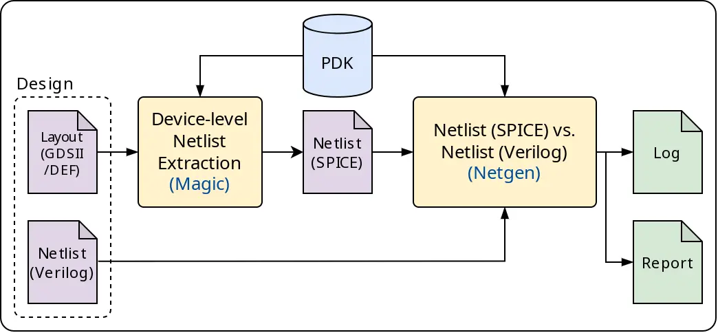
Fig. 31 LVS flow — SPICE extraction from layout feeds into Netgen comparison against the power-aware netlist.
Step 1 — SPICE Extraction (Magic.SpiceExtraction): Magic reverse-engineers the
electrical connectivity from the GDSII, producing a .spice file — the “as-built”
wiring diagram of the physical design.
Step 2 — Netlist Comparison (Netgen.LVS): Netgen compares Circuit 1 (extracted
SPICE — the as-built reality) against Circuit 2 (the power-aware .pnl netlist — the
as-planned intent). The comparison covers all logical pins, power pins (VPWR/VGND),
and substrate bias pins (VNB/VPB) required by the SkyWater 130nm PDK for latch-up
prevention.
7. Running the Physical Signoff Flow
With all signoff prep violations resolved via ECO, run the physical signoff steps starting from the ECO run’s final state:
[nix-shell:~]$ librelane \
    ~/Silicon-Sprint-AUC/openlane/aes_wb_wrapper/config.json \
    --run-tag classic_flow_eco \
    --from Magic.StreamOut \
    --with-initial-state \
    ~/Silicon-Sprint-AUC/openlane/aes_wb_wrapper/runs/classic_flow_eco/14-openroad-irdropreport/state_out.json
When all steps complete, the terminal prints the final signoff summary:
 Antenna
Passed ✅
 LVS
Passed ✅
 DRC
Passed ✅
8. Physical Signoff Results
8.1 DRC Report
Location: runs/classic_flow_eco/64-magic-drc/reports/drc.magic.rpt
aes_wb_wrapper
----------------------------------------
[INFO] COUNT: 0
[INFO] Should be divided by 3 or 4
DRC: Clean Pass
COUNT: 0 confirms zero Design Rule violations. The ECO buffers were placed and
routed without introducing any new geometric conflicts. The aes_wb_wrapper layout
is fully compliant with all SkyWater 130nm manufacturing constraints and is ready
for tape-out.
Note: The “Should be divided by 3 or 4” message is a Magic-internal counting normalisation — a normalised count of 0 is an unambiguous clean result.
8.2 LVS Report
Location: runs/classic_flow_eco/70-netgen-lvs/reports/lvs.netgen.rpt
A representative subcircuit comparison for an AND4 gate:
Subcircuit pins:
Circuit 1: sky130_fd_sc_hd__and4_4         |Circuit 2: sky130_fd_sc_hd__and4_4
-------------------------------------------|-------------------------------------------
A                                          |A
B                                          |B
C                                          |C
D                                          |D
VGND                                       |VGND
VNB                                        |VNB
VPB                                        |VPB
VPWR                                       |VPWR
X                                          |X
Circuit 1 (left) — extracted SPICE netlist from the physical GDSII (as-built).
Circuit 2 (right) — power-aware .pnl synthesis netlist (as-planned).
Every pin matches identically — logical I/O (A, B, C, D, X), power (VPWR/VGND),
and substrate bias (VNB/VPB). The ECO-inserted buf_4 cells are present and
correctly wired in both circuits.
Cell pin lists are equivalent.
Device classes aes_wb_wrapper and aes_wb_wrapper are equivalent.
Final result: Circuits match uniquely.
LVS: Circuits Match Uniquely
“Match” — physical connections are logically identical to the netlist. “Uniquely” — Netgen found no topological symmetry requiring ambiguity resolution. Every one of the 27,332+ nets across all 135,744+ instances is proven to be connected exactly where the synthesis netlist specifies. No shorts, opens, or connectivity errors were introduced — including by the ECO buffer insertion and re-routing.
9. Final Output Directory
When the signoff flow completes, LibreLane consolidates all deliverables into the
final/ directory:
runs/classic_flow_eco/final/
├── def/           ← Design Exchange Format (ASCII placement + routing)
├── gds/           ← GDSII layout (Magic) — primary fabrication file
├── klayout_gds/   ← GDSII layout (KLayout) — XOR-verified copy
├── lef/           ← LEF abstract for hierarchical SoC integration
├── lib/           ← Liberty timing models (one per PVT corner)
├── nl/            ← Structural gate-level netlist (no power pins)
├── pnl/           ← Power-aware netlist (with VPWR/VGND pins)
├── odb/           ← OpenROAD binary database
├── sdc/           ← Timing constraints applied at signoff
├── sdf/           ← Standard Delay Format (per-corner, for simulation)
├── spef/          ← Parasitic data (max/nom/min SPEF files)
├── spice/         ← Electrical netlist extracted from layout (for LVS)
├── vh/            ← Verilog header — blackbox stub for top-level synthesis
├── mag/ mag_gds/  ← Magic layout and GDS files
├── json_h/        ← JSON header for design metadata
├── metrics.csv    ← Final area, power, wire length, density summary
└── metrics.json   ← Machine-readable version of metrics
Format |
Extension |
Purpose |
|---|---|---|
GDSII |
|
Fabrication master — submitted to the foundry. |
LEF |
|
Integration abstract for top-level SoC place-and-route. |
Liberty |
|
Timing model for higher-level synthesis tools. |
SPEF |
|
Parasitic data for post-layout simulation. |
Verilog Header |
|
Blackbox port-list stub for top-level synthesis. |
Power Netlist |
|
Power-aware netlist for LVS and system power simulation. |
SDF |
|
RC delays back-annotated per gate for timing-accurate simulation. |
ODB |
|
OpenROAD binary database for flow re-entry. |
Metrics |
|
Quantitative signoff record — area, power, wire length, density. |
- GDSII
Graphic Database System II. The standard binary layout format delivered to the foundry for fabrication.
- DRC
Design Rule Check. Verification that the layout conforms to foundry manufacturing constraints.
- LVS
Layout vs. Schematic. Verification that the physical layout is electrically equivalent to the design netlist.
- SPICE
Simulation Program with Integrated Circuit Emphasis. The file format produced by Magic extraction for LVS.
- LEF
Library Exchange Format. Physical interface description of a macro — boundary, pins, and blockages.
- PDN
Power Distribution Network. The metal grid delivering VDD and GND to every standard cell.
- PnR
Place and Route. Standard cell placement and signal wire routing.
- STA
Static Timing Analysis. Exhaustive path-by-path timing verification against declared constraints.
- PVT
Process, Voltage, Temperature. The three axes of semiconductor variation, analysed through multiple corners.
- WNS
Worst Negative Slack. The largest magnitude of negative slack across all failing timing paths.
- TNS
Total Negative Slack. The sum of all negative slack values across every failing path.
- SDC
Synopsys Design Constraints. Tcl-based timing and clocking constraints.