Module 1: LibreLane Flow & Execution to PDN
Prerequisites
Before proceeding, ensure your environment is fully prepared by completing all steps in Module 0. Your repository must be cloned and the Nix-shell verified before starting the ASIC flow.
Table of Contents
1. RTL Integration — The Wishbone Wrapper
Before beginning the ASIC flow, we must bridge the gap between the AES Core and the
Caravel SoC. This is accomplished by encapsulating the design inside a Wishbone
Wrapper (aes_wb_wrapper.v) — a standardised communication adapter that allows the
Caravel CPU to exchange data with the AES encryption engine using a well-defined bus
protocol.
Note
In later modules, we will demonstrate how to integrate this complete unit into the User Project Wrapper. For now, the objective is to ensure the AES logic is “Wishbone-ready.”
Why Do We Need the Wishbone Wrapper?
Reason |
Explanation |
|---|---|
Standardisation |
Adheres to the Wishbone protocol natively understood by the Caravel harness. |
Addressability |
Assigns the AES core a specific memory address so the CPU can locate it on the bus. |
Control |
Allows the system to independently reset or clock the AES core. |
1.1 Architectural Overview
Before writing any code, study the block diagram below. It illustrates how the AES Core
is encapsulated within the Wishbone Wrapper. The wrapper serves as the translation layer,
converting standard Wishbone bus signals — such as wbs_stb_i and wbs_dat_i — into the
control signals the AES engine requires.
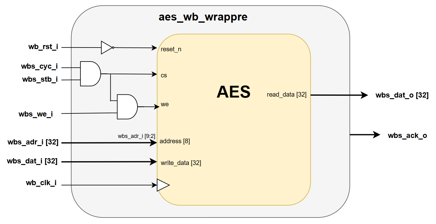
Fig. 1 Block diagram of aes_wb_wrapper
1.2 Creating the Verilog Wrapper
Follow the steps below to create the interface file that bridges the AES logic with the Wishbone bus.
Step 1 — Initialize the Wrapper File
We use gedit (a lightweight graphical text editor) to create the wrapper file. If the file does not already exist, it will be initialized as an empty document.
$ gedit ~/Silicon-Sprint-AUC/verilog/rtl/aes_wb_wrapper.v
Step 2 — Add the Verilog Implementation
Once the editor opens, paste the Wishbone wrapper implementation into the file. This module manages all communication between the Caravel SoC and the AES core. After pasting, save the file and close the editor.
aes_wb_wrapper.v
 1// SPDX-FileCopyrightText: 2020 Efabless Corporation
 2//
 3// Licensed under the Apache License, Version 2.0 (the "License");
 4// you may not use this file except in compliance with the License.
 5// You may obtain a copy of the License at
 6//
 7//      http://www.apache.org/licenses/LICENSE-2.0
 8//
 9// Unless required by applicable law or agreed to in writing, software
10// distributed under the License is distributed on an "AS IS" BASIS,
11// WITHOUT WARRANTIES OR CONDITIONS OF ANY KIND, either express or implied.
12// See the License for the specific language governing permissions and
13// limitations under the License.
14// SPDX-License-Identifier: Apache-2.0
15
16`default_nettype none
17
18module aes_wb_wrapper (
19`ifdef USE_POWER_PINS
20    inout VPWR,
21    inout VGND,
22`endif
23
24    // Wishbone Slave ports (WB MI A)
25    input wb_clk_i,
26    input wb_rst_i,
27    input wbs_stb_i,
28    input wbs_cyc_i,
29    input wbs_we_i,
30    input [3:0] wbs_sel_i,
31    input [31:0] wbs_dat_i,
32    input [31:0] wbs_adr_i,
33    output wbs_ack_o,
34    output [31:0] wbs_dat_o
35);
36
37    wire valid;
38    wire write_enable;
39    wire read_enable;
40
41    reg wbs_ack_o_reg;
42
43    assign valid = wbs_cyc_i && wbs_stb_i;
44    assign write_enable = wbs_we_i && valid;
45    assign read_enable = ~wbs_we_i && valid;
46
47    aes aes(
48        // Clock and reset.
49        .clk(wb_clk_i),
50        .reset_n(!wb_rst_i),
51
52        // Control.
53        .cs(wbs_cyc_i && wbs_stb_i),
54        .we(write_enable),
55
56        // Data ports.
57        .address(wbs_adr_i[9:2]),
58        .write_data(wbs_dat_i),
59        .read_data(wbs_dat_o)
60    );
61
62    // Ack logic
63    always @(posedge wb_clk_i or posedge wb_rst_i) begin
64        if (wb_rst_i)
65            wbs_ack_o_reg <= 1'b0;
66        else if (wbs_cyc_i && wbs_stb_i && ~wbs_ack_o_reg)
67            wbs_ack_o_reg <= 1'b1;
68        else
69            wbs_ack_o_reg <= 1'b0;
70    end
71
72    assign wbs_ack_o = wbs_ack_o_reg;
73
74endmodule
75
76`default_nettype none
2. The LibreLane Classic Flow
The LibreLane Classic Flow is a sequential, automated RTL-to-GDSII pipeline built entirely on open-source EDA tools. Each phase of ASIC design — from logic verification through physical signoff — is handled by a specialised tool within a single unified environment.
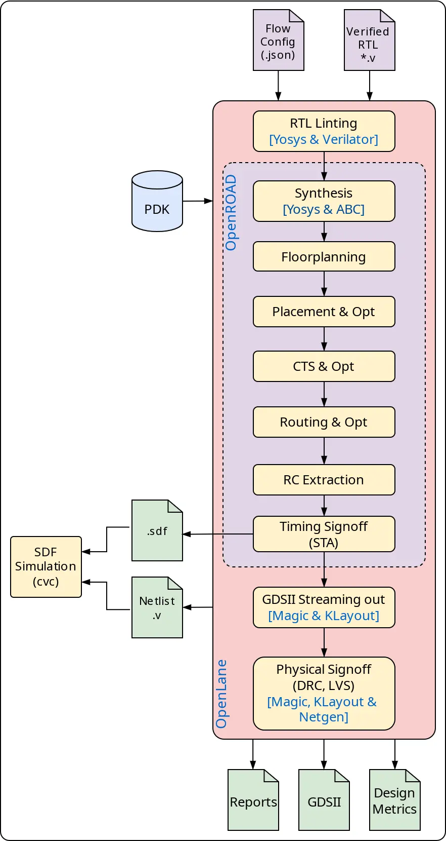
Fig. 2 LibreLane RTL-to-GDSII Flow
Key Concept — Deterministic Execution
The Classic flow is deterministic and repeatable. Every run follows the same ordered sequence of steps, making it the ideal starting point for learning the full ASIC design process.
2.1 Flow Step Reference
Each step in the flow carries a unique Step ID in the format ToolName.StepName.
These IDs are consumed directly by the librelane command line to start, stop, or skip
individual stages (see Section 5).
Stage |
Step Description |
Step ID |
|---|---|---|
Logic Verification |
RTL Linting with Verilator |
|
Check Timing Constructs |
|
|
Check for Lint Errors |
|
|
Check for Lint Warnings |
|
|
Synthesis |
Generate Netlist JSON Header |
|
RTL Synthesis and Tech Mapping |
|
|
Check for Unmapped Cells |
|
|
Logic Synthesis Checks |
|
|
Netlist Assign Statement Check |
|
|
Floorplanning |
Validate SDC Constraints |
|
Validate Macro Instances |
|
|
Pre-PnR Static Timing Analysis |
|
|
Initial Floorplan Generation |
|
|
Dump Resistance/Capacitance Values |
|
|
Check Macro Antenna Properties |
|
|
Macro Power Connections |
|
|
Manual Macro Placement |
|
|
Cut Rows for Macro Sites |
|
|
Tap and Endcap Cell Insertion |
|
|
Power Grid |
Add PDN Obstructions |
|
Power Distribution Network Generation |
|
|
Remove PDN Obstructions |
|
|
Add Routing Obstructions |
|
|
Placement |
Global Placement (Skip IO) |
|
IO Pin Placement |
|
|
Custom IO Pin Placement |
|
|
Apply DEF Template |
|
|
Global Placement |
|
|
Write Verilog Header |
|
|
Power Grid Violation Check |
|
|
Mid-PnR Static Timing Analysis (1) |
|
|
Design Repair (Post-GPL) |
|
|
Manual Global Placement |
|
|
Detailed Placement |
|
|
CTS |
Clock Tree Synthesis |
|
Mid-PnR Static Timing Analysis (2) |
|
|
Resizer Timing (Post-CTS) |
|
|
Mid-PnR Static Timing Analysis (3) |
|
|
Routing |
Global Routing |
|
Initial Antenna Check |
|
|
Design Repair (Post-GRT) |
|
|
Diodes on Ports |
|
|
Heuristic Diode Insertion |
|
|
Antenna Repair |
|
|
Resizer Timing (Post-GRT) |
|
|
Mid-PnR Static Timing Analysis (4) |
|
|
Detailed Routing |
|
|
Remove Routing Obstructions |
|
|
Final Antenna Check |
|
|
Detailed Routing DRC Check |
|
|
Report Disconnected Pins |
|
|
Disconnected Pins Check |
|
|
Report Wire Length |
|
|
Wire Length Check |
|
|
Signoff Prep |
Fill Cell Insertion |
|
Cell Frequency Tables |
|
|
Parasitics Extraction |
|
|
Post-PnR STA |
|
|
IR Drop Reporting |
|
|
Physical Signoff |
GDSII Stream Out (Magic) |
|
GDSII Stream Out (KLayout) |
|
|
KLayout Render |
|
|
Write Macro LEF |
|
|
Check Design Antenna Properties |
|
|
XOR GDS Comparison |
|
|
XOR Comparison Check |
|
|
Physical DRC (Magic) |
|
|
Physical DRC (KLayout) |
|
|
Magic DRC Check |
|
|
KLayout DRC Check |
|
|
SPICE Netlist Extraction |
|
|
Illegal Overlap Check |
|
|
Layout vs. Schematic (LVS) |
|
|
LVS Comparison Check |
|
|
Formal Equivalence Check |
|
|
Setup Violations Check |
|
|
Hold Violations Check |
|
|
Max Slew Violations Check |
|
|
Max Cap Violations Check |
|
|
Final Manufacturability Report |
|
3. Setting Up the Design Environment
This section follows an Iterative Configuration Strategy: we begin with the minimum required settings, execute the flow, analyse the generated reports, and progressively refine the configuration based on observed results.
Step 1 — Create the Design Directory
Create the dedicated folder where LibreLane will look for your config.json:
$ mkdir -p ~/Silicon-Sprint-AUC/openlane/aes_wb_wrapper
Step 2 — Define Timing Constraints (SDC Files)
To achieve timing closure on a complex design like the AES accelerator, it is
strongly recommended to provide design-specific SDC files rather than relying on
the tool’s auto-generated defaults. This is controlled via the PNR_SDC_FILE and
SIGNOFF_SDC_FILE configuration variables.
Key Concept — The Timing Contract
SDC files function as a “timing contract” between your RTL and the physical implementation tools. They declare the clock frequency, multicycle paths, and I/O timing requirements that OpenROAD must satisfy during PnR.
Note
How the two SDC files work together:
The pnr.sdc file is applied throughout the entire implementation flow — including
Placement, CTS, and Routing — to maintain high signal integrity during physical
implementation. The signoff.sdc file is only used at the final signoff stage for
the ultimate timing and DRC validation.
This two-file strategy is intentional:
Restrictive PnR:
pnr.sdcapplies a strict 0.75 ns maximum transition limit. This forces the engine to work aggressively during placement and routing, resolving the vast majority of slew violations before signoff.Signoff Relaxation:
signoff.sdcapplies a relaxed 1.5 ns transition limit, consistent with thesky130_fd_sc_hdlibrary characterisation boundary. Since the tool has already fixed violations against the tighter constraint during PnR, most slew violations disappear at signoff — producing a clean final timing report.
PnR Constraint File (pnr.sdc)
Applied during all implementation steps (Placement, CTS, Routing). Sets the clock period, defines a strict 0.75 ns maximum transition, specifies multicycle paths, and establishes realistic clock latency and I/O delay values based on the Caravel SoC environment.
$ gedit ~/Silicon-Sprint-AUC/openlane/aes_wb_wrapper/pnr.sdc
Paste the following code into the editor and save:
pnr.sdc
#------------------------------------------#
# Design Constraints
#------------------------------------------#

# Clock network
set clk_input wb_clk_i
create_clock [get_ports $clk_input] -name clk -period 25
puts "\[INFO\]: Creating clock {clk} for port $clk_input with period: 25"

# Clock non-idealities
set_propagated_clock [get_clocks {clk}]
set_clock_uncertainty 0.12 [get_clocks {clk}]
puts "\[INFO\]: Setting clock uncertainty to: 0.12"

# Maximum transition time for the design nets
set_max_transition 0.75 [current_design]
puts "\[INFO\]: Setting maximum transition to: 0.75"

# Maximum fanout
set_max_fanout 16 [current_design]
puts "\[INFO\]: Setting maximum fanout to: 16"

# Timing paths delays derate
set_timing_derate -early [expr {1-0.07}]
set_timing_derate -late [expr {1+0.07}]

# Multicycle paths
set_multicycle_path -setup 2 -through [get_ports {wbs_ack_o}]
set_multicycle_path -hold 1  -through [get_ports {wbs_ack_o}]
set_multicycle_path -setup 2 -through [get_ports {wbs_cyc_i}]
set_multicycle_path -hold 1  -through [get_ports {wbs_cyc_i}]
set_multicycle_path -setup 2 -through [get_ports {wbs_stb_i}]
set_multicycle_path -hold 1  -through [get_ports {wbs_stb_i}]

#------------------------------------------#
# Retrieved Constraints then modified
#------------------------------------------#

# Clock source latency
set usr_clk_max_latency 4.57
set usr_clk_min_latency 4.11
set clk_max_latency 5.70
set clk_min_latency 4.40
set_clock_latency -source -max $clk_max_latency [get_clocks {clk}]
set_clock_latency -source -min $clk_min_latency [get_clocks {clk}]
puts "\[INFO\]: Setting clock latency range: $clk_min_latency : $clk_max_latency"

# Clock input Transition
set_input_transition 0.61 [get_ports $clk_input]

# Input delays
set_input_delay -max 3.27 -clock [get_clocks {clk}] [get_ports {wbs_sel_i[*]}]
set_input_delay -max 3.84 -clock [get_clocks {clk}] [get_ports {wbs_we_i}]
set_input_delay -max 3.99 -clock [get_clocks {clk}] [get_ports {wbs_adr_i[*]}]
set_input_delay -max 4.23 -clock [get_clocks {clk}] [get_ports {wbs_stb_i}]
set_input_delay -max 4.71 -clock [get_clocks {clk}] [get_ports {wbs_dat_i[*]}]
set_input_delay -max 4.84 -clock [get_clocks {clk}] [get_ports {wbs_cyc_i}]
set_input_delay -min 0.50 -clock [get_clocks {clk}] [get_ports {wbs_adr_i[*]}]
set_input_delay -min 0.94 -clock [get_clocks {clk}] [get_ports {wbs_dat_i[*]}]
set_input_delay -min 1.09 -clock [get_clocks {clk}] [get_ports {wbs_sel_i[*]}]
set_input_delay -min 1.55 -clock [get_clocks {clk}] [get_ports {wbs_we_i}]
set_input_delay -min 1.20 -clock [get_clocks {clk}] [get_ports {wbs_cyc_i}]
set_input_delay -min 1.46 -clock [get_clocks {clk}] [get_ports {wbs_stb_i}]

# Reset input delay
set_input_delay [expr 25 * 0.5] -clock [get_clocks {clk}] [get_ports {wb_rst_i}]

# Input Transition
set_input_transition -max 0.14  [get_ports {wbs_we_i}]
set_input_transition -max 0.15  [get_ports {wbs_stb_i}]
set_input_transition -max 0.17  [get_ports {wbs_cyc_i}]
set_input_transition -max 0.18  [get_ports {wbs_sel_i[*]}]
set_input_transition -max 0.84  [get_ports {wbs_dat_i[*]}]
set_input_transition -max 0.92  [get_ports {wbs_adr_i[*]}]
set_input_transition -min 0.07  [get_ports {wbs_adr_i[*]}]
set_input_transition -min 0.07  [get_ports {wbs_dat_i[*]}]
set_input_transition -min 0.09  [get_ports {wbs_cyc_i}]
set_input_transition -min 0.09  [get_ports {wbs_sel_i[*]}]
set_input_transition -min 0.09  [get_ports {wbs_we_i}]
set_input_transition -min 0.15  [get_ports {wbs_stb_i}]

# Output delays
set_output_delay -max 3.72 -clock [get_clocks {clk}] [get_ports {wbs_dat_o[*]}]
set_output_delay -max 8.51 -clock [get_clocks {clk}] [get_ports {wbs_ack_o}]
set_output_delay -min 1.03 -clock [get_clocks {clk}] [get_ports {wbs_dat_o[*]}]
set_output_delay -min 1.27 -clock [get_clocks {clk}] [get_ports {wbs_ack_o}]

# Output loads
set_load 0.19 [all_outputs]
Signoff Constraint File (signoff.sdc)
Applied only at the final signoff STA stage. Uses a relaxed 1.5 ns maximum transition
limit and slightly less pessimistic timing derate values (±5% vs ±7% in pnr.sdc),
reflecting a more realistic assessment of the manufactured silicon’s operating envelope.
$ gedit ~/Silicon-Sprint-AUC/openlane/aes_wb_wrapper/signoff.sdc
Paste the following code into the editor and save:
signoff.sdc
#------------------------------------------#
# Design Constraints
#------------------------------------------#

# Clock network
set clk_input wb_clk_i
create_clock [get_ports $clk_input] -name clk -period 25
puts "\[INFO\]: Creating clock {clk} for port $clk_input with period: 25"

# Clock non-idealities
set_propagated_clock [get_clocks {clk}]
set_clock_uncertainty 0.1 [get_clocks {clk}]
puts "\[INFO\]: Setting clock uncertainty to: 0.1"

# Maximum transition time for the design nets
set_max_transition 1.5 [current_design]
puts "\[INFO\]: Setting maximum transition to: 1.5"

# Maximum fanout
set_max_fanout 16 [current_design]
puts "\[INFO\]: Setting maximum fanout to: 16"

# Timing paths delays derate
set_timing_derate -early [expr {1-0.05}]
set_timing_derate -late [expr {1+0.05}]
puts "\[INFO\]: Setting timing derate to: [expr {0.05 * 100}] %"

# Multicycle paths
set_multicycle_path -setup 2 -through [get_ports {wbs_ack_o}]
set_multicycle_path -hold 1  -through [get_ports {wbs_ack_o}]
set_multicycle_path -setup 2 -through [get_ports {wbs_cyc_i}]
set_multicycle_path -hold 1  -through [get_ports {wbs_cyc_i}]
set_multicycle_path -setup 2 -through [get_ports {wbs_stb_i}]
set_multicycle_path -hold 1  -through [get_ports {wbs_stb_i}]

#------------------------------------------#
# Retrieved Constraints
#------------------------------------------#

# Clock source latency
set usr_clk_max_latency 4.57
set usr_clk_min_latency 4.11
set clk_max_latency 5.57
set clk_min_latency 4.65
set_clock_latency -source -max $clk_max_latency [get_clocks {clk}]
set_clock_latency -source -min $clk_min_latency [get_clocks {clk}]
puts "\[INFO\]: Setting clock latency range: $clk_min_latency : $clk_max_latency"

# Clock input Transition
set_input_transition 0.61 [get_ports $clk_input]

# Input delays
set_input_delay -max 3.17 -clock [get_clocks {clk}] [get_ports {wbs_sel_i[*]}]
set_input_delay -max 3.74 -clock [get_clocks {clk}] [get_ports {wbs_we_i}]
set_input_delay -max 3.89 -clock [get_clocks {clk}] [get_ports {wbs_adr_i[*]}]
set_input_delay -max 4.13 -clock [get_clocks {clk}] [get_ports {wbs_stb_i}]
set_input_delay -max 4.61 -clock [get_clocks {clk}] [get_ports {wbs_dat_i[*]}]
set_input_delay -max 4.74 -clock [get_clocks {clk}] [get_ports {wbs_cyc_i}]
set_input_delay -min 0.79 -clock [get_clocks {clk}] [get_ports {wbs_adr_i[*]}]
set_input_delay -min 1.04 -clock [get_clocks {clk}] [get_ports {wbs_dat_i[*]}]
set_input_delay -min 1.19 -clock [get_clocks {clk}] [get_ports {wbs_sel_i[*]}]
set_input_delay -min 1.65 -clock [get_clocks {clk}] [get_ports {wbs_we_i}]
set_input_delay -min 1.69 -clock [get_clocks {clk}] [get_ports {wbs_cyc_i}]
set_input_delay -min 1.86 -clock [get_clocks {clk}] [get_ports {wbs_stb_i}]

# Reset input delay
set_input_delay [expr 25 * 0.5] -clock [get_clocks {clk}] [get_ports {wb_rst_i}]

# Input Transition
set_input_transition -max 0.14  [get_ports {wbs_we_i}]
set_input_transition -max 0.15  [get_ports {wbs_stb_i}]
set_input_transition -max 0.17  [get_ports {wbs_cyc_i}]
set_input_transition -max 0.18  [get_ports {wbs_sel_i[*]}]
set_input_transition -max 0.84  [get_ports {wbs_dat_i[*]}]
set_input_transition -max 0.92  [get_ports {wbs_adr_i[*]}]
set_input_transition -min 0.07  [get_ports {wbs_adr_i[*]}]
set_input_transition -min 0.07  [get_ports {wbs_dat_i[*]}]
set_input_transition -min 0.09  [get_ports {wbs_cyc_i}]
set_input_transition -min 0.09  [get_ports {wbs_sel_i[*]}]
set_input_transition -min 0.09  [get_ports {wbs_we_i}]
set_input_transition -min 0.15  [get_ports {wbs_stb_i}]

# Output delays
set_output_delay -max 3.62 -clock [get_clocks {clk}] [get_ports {wbs_dat_o[*]}]
set_output_delay -max 8.41 -clock [get_clocks {clk}] [get_ports {wbs_ack_o}]
set_output_delay -min 1.13 -clock [get_clocks {clk}] [get_ports {wbs_dat_o[*]}]
set_output_delay -min 1.37 -clock [get_clocks {clk}] [get_ports {wbs_ack_o}]

# Output loads
set_load 0.19 [all_outputs]
The key differences between the two files are summarised below:
Constraint |
|
|
|---|---|---|
Maximum Transition |
0.75 ns (strict) |
1.5 ns (library limit) |
Timing Derate |
±7% |
±5% |
Clock Uncertainty |
0.12 ns |
0.10 ns |
Clock Latency (max) |
5.70 ns |
5.57 ns |
Step 3 — Create the Base Configuration File
The config.json file is the master instruction set for the LibreLane flow. We begin
with the minimum required settings and will expand it progressively in the steps that follow.
Create and open the file:
$ gedit ~/Silicon-Sprint-AUC/openlane/aes_wb_wrapper/config.json
Paste the following base configuration:
{
    "DESIGN_NAME": "aes_wb_wrapper",
    "PDN_MULTILAYER": false,
    "CLOCK_PORT": "wb_clk_i",
    "CLOCK_PERIOD": 25,
    "VERILOG_FILES": [
        "dir::../../../secworks_aes/src/rtl/*.v",
        "dir::../../verilog/rtl/aes_wb_wrapper.v"
    ],
    "FP_CORE_UTIL": 40,
    "RT_MAX_LAYER": "met4",
    "PNR_SDC_FILE": "dir::pnr.sdc",
    "SIGNOFF_SDC_FILE": "dir::signoff.sdc"
}
Note
FP_CORE_UTIL is set to 40% (the default is 50%). This lower utilisation leaves
more routing headroom for the AES core’s dense combinational logic, reducing the risk
of routing congestion during placement and routing.
Configuration Variable Reference
Variable |
Value |
Description |
|---|---|---|
|
|
Must match the top-level Verilog module name exactly. |
|
(glob path) |
All RTL source files. The |
|
|
The RTL port designated as the primary clock input. |
|
|
Clock period in nanoseconds — 25 ns = 40 MHz. |
|
|
Restricts the PDN to Metal 4 vertical straps only, leaving Metal 5 clear for Caravel top-level integration. See Section 4.3. |
|
|
Core utilisation percentage. Set to 40% (default: 50%) for routing headroom. |
|
|
Restricts all signal routing to Metal 4 and below, leaving Metal 5 clear for the top-level PDN. |
Warning
Minimum Required Variables
Every LibreLane design configuration must include the following four variables at a minimum. The flow will fail at initialisation if any are absent:
DESIGN_NAMEVERILOG_FILESCLOCK_PERIODCLOCK_PORT
Note that PNR_SDC_FILE and SIGNOFF_SDC_FILE will be added once we have confirmed
the best synthesis strategy in Section 6.
4. RTL-to-Power-Grid Configuration Reference
This section documents the key config.json parameters for synthesis, floorplanning, and
power distribution. These are provided as a reference — not all are used in this module.
Values are tuned progressively as the flow matures across modules.
4.1 Logic Synthesis Configuration Reference
Synthesis maps your RTL to the SkyWater 130nm (sky130_fd_sc_hd) standard cell library.
The parameters below govern the trade-off between gate count and achievable clock frequency.
Parameter |
Type |
Description |
Default |
|---|---|---|---|
|
|
Selects the ABC logic synthesis strategy. |
|
|
|
Controls hierarchy handling: |
|
|
|
Enables automated cell buffering within ABC to improve signal integrity and timing margins. |
|
|
|
Enables ABC cell sizing to optimise gate drive strength. |
|
|
|
Allows Yosys to identify and merge shareable hardware resources (e.g., adders) to reduce total area. |
|
|
|
Generates human-readable instance names in the netlist. Useful for debugging; may produce very long names. |
|
|
|
Performs RTL elaboration only, without technology mapping. Use if the Verilog is already gate-level. |
|
|
|
Specifies the macro used to guard power/ground connections in the RTL. |
|
|
|
Quits the flow immediately if synthesis check errors are found — specifically combinational loops or wires with no drivers. Catching these early prevents hard-to-debug downstream failures. |
|
|
|
Emits an error (rather than a warning) if assign statements are found in the post-synthesis netlist, which may indicate incomplete technology mapping. |
|
4.2 Floorplan Configuration Reference
These parameters define the physical boundaries of the AES core. Correct floorplan settings ensure the macro fits within the designated User Project area while preserving adequate routing resources.
Parameter |
Type |
Description |
Default |
|---|---|---|---|
|
|
Core utilisation percentage. |
|
|
|
Core aspect ratio (height ÷ width). A value of 1 creates a square floorplan. |
|
|
|
|
|
|
|
Fixed die boundary as |
|
|
|
Explicit core area boundary. Must be paired with |
|
|
|
Bottom core margin in multiples of site heights. Ignored if |
|
|
|
Top core margin in multiples of site heights. |
|
|
|
Left core margin in multiples of site widths. |
|
|
|
Right core margin in multiples of site widths. |
|
Relative vs. Absolute Floorplan Sizing
Relative Sizing ("FP_SIZING": "relative") — The default mode. LibreLane calculates
chip area automatically from gate count and FP_CORE_UTIL. Use this for initial iterations
to find the smallest feasible footprint.
Absolute Sizing ("FP_SIZING": "absolute") — Mandatory for fixed-size projects such
as the Caravel User Project. Physical coordinates are explicitly declared via DIE_AREA
(e.g., 0 0 2920 3520), ensuring the AES core fits precisely into the pre-defined silicon
cavity of the SoC.
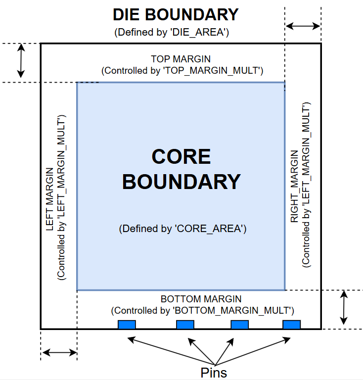
Fig. 3 Floorplan boundary and margin visualisation
4.3 Power Distribution Network (PDN) Configuration Reference
The PDN is the grid of metal conductors delivering VDD and GND to every
standard cell in the design. LibreLane supports two fundamentally different methods
for constructing the PDN of a macro, and the choice between them affects which metal
layers are available for signal routing.
PDN Method 1 — Hierarchical
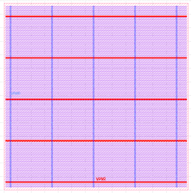
In the Hierarchical method, power is delivered through stacked metal straps: each level of the design hierarchy uses a different metal layer for power straps, and the macro boundary is deliberately kept clear of the topmost used layer so that the parent-level integration can connect through vias.
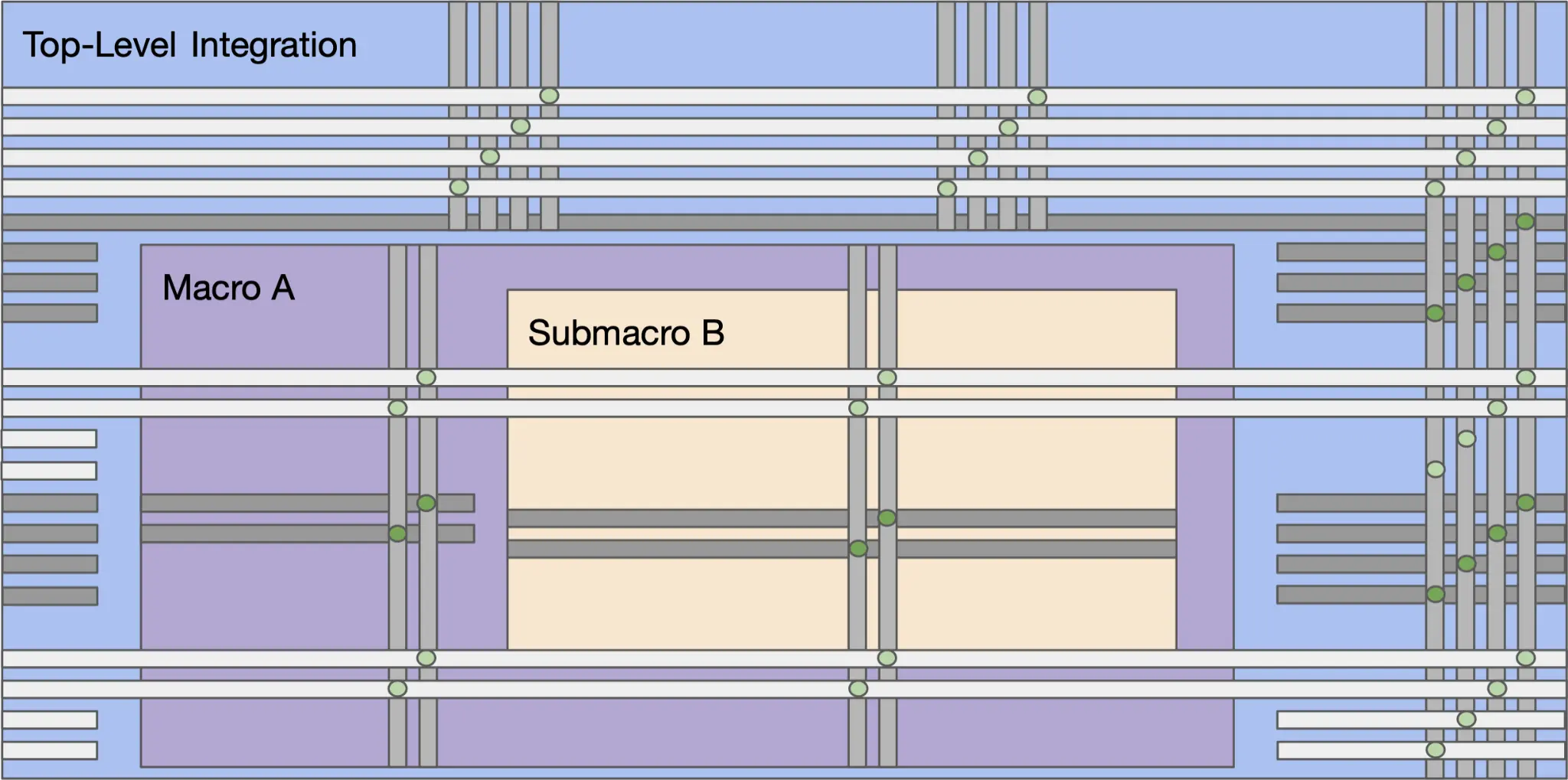
Fig. 4 Hierarchical PDN — each level of hierarchy gives up the topmost metal layer so the level above can connect through.
The rule is simple: if your macro will be placed inside a top-level wrapper that uses met5 for horizontal power straps, your macro must not use met5 — for either PDN or signal routing.
Critical Parameters for Hierarchical Method
When using the hierarchical method for a macro that will be integrated into the OpenFrame multiproject wrapper, two parameters must be set together:
PDN_MULTILAYER: false— Restricts the macro’s PDN to vertical straps on Metal 4 only. Metal 5 is left completely clear for the top-level wrapper’s horizontal power straps.RT_MAX_LAYER: "met4"— Prevents the router from placing any signal wire on Metal 5. Without this, detailed routing may use met5 for signal wires, creating DRC conflicts with the wrapper’s power grid.
Omitting either parameter will result in met5 conflicts and fatal DRC violations when the macro is integrated into the top level.

PDN Method 2 — Ring
In the Ring method, a closed power ring is built around the perimeter of the macro core area. This ring is connected to the top-level integration by abutment — the top level connects to the ring edges rather than running straps through the macro.
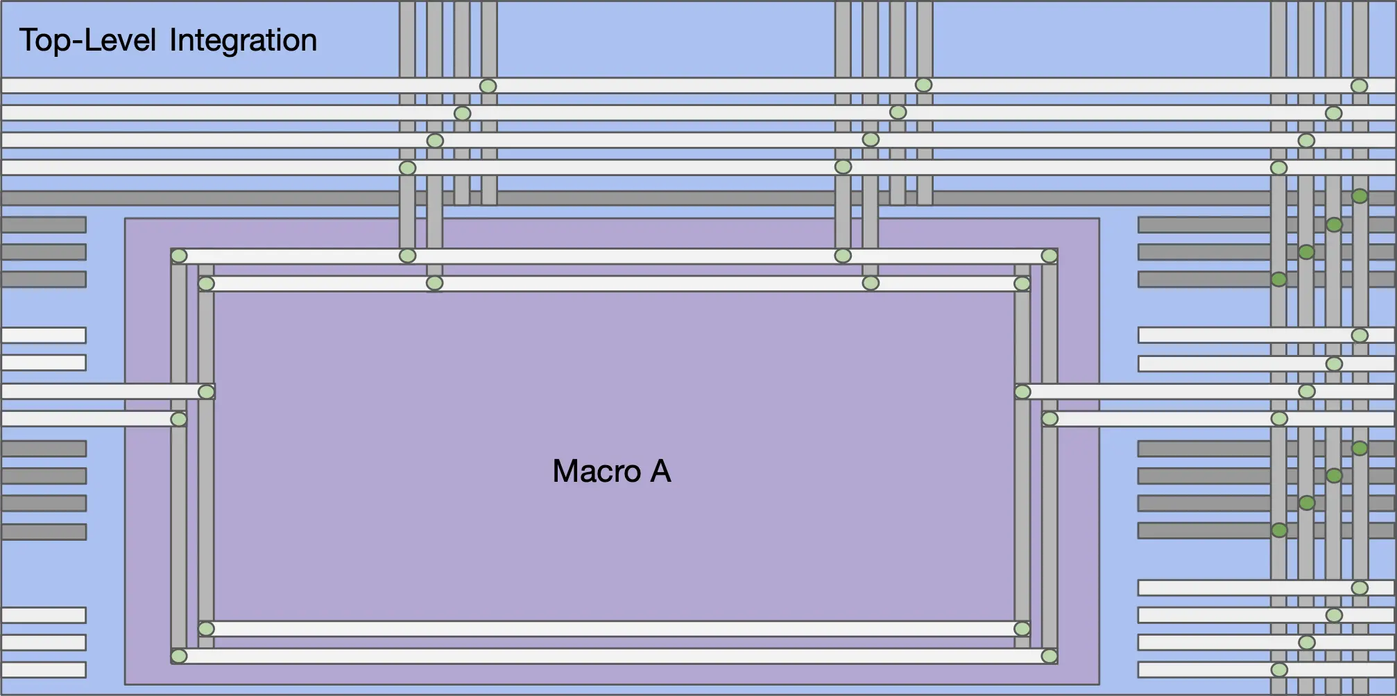
Fig. 7 Ring PDN — a closed power ring surrounds the core; the full metal layer stack is available for internal routing.
The key advantage is that the macro can use all available metal layers for signal routing — including met5 — because the power ring does not depend on reserving the topmost layer for vertical strap continuity. The trade-off is that the ring occupies additional area around the core perimeter.
"PDN_CORE_RING": true
PDN Control Parameters
Parameter |
Type |
Description |
Default |
|---|---|---|---|
|
|
Generates both vertical (M4) and horizontal (M5) straps. Set |
|
|
|
Enables the ring method — builds a power ring around the core perimeter. |
|
|
|
Width of vertical ring segments. |
|
|
|
Width of horizontal ring segments. |
|
|
|
Spacing between the VDD and GND vertical ring straps. |
|
|
|
Spacing between the VDD and GND horizontal ring straps. |
|
|
|
Offset of the vertical ring from the core boundary. |
|
|
|
Offset of the horizontal ring from the core boundary. |
|
|
|
Enables Metal 1 standard cell power rails across every cell row. |
|
|
|
Prevents removal of metal stubs not connected to macros. |
|
|
|
Horizontal keep-out distance around macros. |
|
|
|
Vertical keep-out distance around macros. |
|
|
|
Custom PDN Tcl configuration file. Uses built-in defaults if not set. |
|
SkyWater 130nm PDN Layer Defaults
Design Element |
Parameter |
Default Value |
Description |
|---|---|---|---|
M1 Rails |
|
0.48 µm |
Standard cell power rail width. |
|
0 |
Starting rail offset. |
|
M4 Vertical Straps |
|
1.6 µm |
Width of vertical power lines. |
|
1.7 µm |
Spacing between parallel vertical straps. |
|
|
153.6 µm |
Centre-to-centre pitch. |
|
|
16.32 µm |
X-axis offset from the left core boundary. |
|
M5 Horizontal Straps |
|
1.6 µm |
Width (active only when |
|
153.18 µm |
Y-axis pitch. |
For further reading, refer to the LibreLane PDN documentation.
5. The librelane Command Syntax
Before issuing any commands, ensure you are inside the Nix shell environment (see Section 6.3).
[nix-shell:~]$ librelane [OPTIONS] [CONFIG_FILE]...
Sequential Flow Controls
Option |
Description |
Example |
|---|---|---|
|
Starts the flow from a specific step. |
|
|
Stops the flow after a specific step completes. |
|
|
Bypasses a specific step during execution. |
|
Run Management Options
Option |
Description |
|---|---|
|
Assigns a custom name to the run directory. Essential for preserving and comparing different runs. |
|
Automatically targets the most recently created run directory. |
|
Overwrites the existing run directory if a matching tag is found. |
|
Resumes a previous flow using a specific |
Flow Configuration Modes (--flow / -f)
Mode |
Description |
|---|---|
|
Standard sequential flow. Predictable, step-by-step — the recommended starting point for learning. |
|
Iterates through all available |
|
Opens the current design state in KLayout for GDSII/DEF inspection. |
|
Opens the design in the OpenROAD GUI for physical analysis. |
6. Run 1: Execution to Power Network (Classic Flow)
In this run, we execute the Classic Flow up to the completion of the PDN. Before doing so, we first identify the best synthesis strategy using the Synthesis Exploration flow.
6.1 Synthesis Exploration
When hardening a new design, it is essential to first identify the optimal synthesis strategy. Synthesis strategies are scripts for the ABC utility that handle fine-grained optimisation and technology mapping. LibreLane provides a dedicated exploration flow that automatically iterates through all available strategies and compares their outcomes.
Tip
It is always recommended to run SynthesisExploration before committing to a full
implementation run. Since AREA strategies minimise footprint while DELAY strategies
optimise timing, the best choice is design-specific and cannot be reliably predicted
in advance.
Entering the Nix Shell
Before running any LibreLane commands, activate the Nix environment to ensure all EDA tools (Yosys, OpenROAD, Magic, etc.) are loaded at the correct versions.
$ nix-shell --pure ~/librelane/shell.nix
Your prompt will change to [nix-shell:~]$, confirming the environment is active.
Tip
Always verify you are inside the Nix shell before invoking librelane. Commands
executed outside the shell may use incompatible system-level tool versions, producing
non-reproducible results.
Run the following command:
[nix-shell:~]$ librelane \
    ~/Silicon-Sprint-AUC/openlane/aes_wb_wrapper/config.json \
    --flow SynthesisExploration \
    --run-tag synexp
The exploration flow tests all nine strategies and prints a ranked summary table. For the
aes_wb_wrapper, the results look as follows:
┏━━━━━━━━━━━━━━━━┳━━━━━━━┳━━━━━━━━━━━━━━━┳━━━━━━━━━━━━━━━━━━━━━━━━━━━━┳━━━━━━━━━━━━━━━━━━━━━━━━┳━━━━━━━━━━━━━━━━━━━━━━━━━━━━┓
┃ SYNTH_STRATEGY ┃ Gates ┃ Area (µm²)    ┃ Worst R2R Setup Slack (ns) ┃ Worst Setup Slack (ns) ┃ Total -ve Setup Slack (ns) ┃
┡━━━━━━━━━━━━━━━━╇━━━━━━━╇━━━━━━━━━━━━━━━╇━━━━━━━━━━━━━━━━━━━━━━━━━━━━╇━━━━━━━━━━━━━━━━━━━━━━━━╇━━━━━━━━━━━━━━━━━━━━━━━━━━━━┩
│ AREA 0         │ 18539 │ 224092.422400 │ -15.910378                 │ -15.910377465847041    │ -19089.359369544294        │
│ AREA 1         │ 18366 │ 223144.012800 │ 1.487758                   │ 1.4877575148500661     │ 0.0                        │
│ AREA 2         │ 18148 │ 220730.448000 │ 1.312014                   │ 1.3120136459736262     │ 0.0                        │
│ AREA 3         │ 34288 │ 309575.657600 │ 10.604188                  │ 8.695160393369793      │ 0.0                        │
│ DELAY 0        │ 25126 │ 292449.232000 │ -15.024117                 │ -15.024117486468324    │ -2965.166315521618         │
│ DELAY 1        │ 26630 │ 303773.843200 │ -11.669471                 │ -11.66947105309875     │ -5372.319416946378         │
│ DELAY 2        │ 26042 │ 296162.793600 │ -5.635439                  │ -5.63543894167321      │ -937.7127677538822         │
│ DELAY 3        │ 24930 │ 290193.318400 │ -17.302505                 │ -17.30250480754339     │ -3854.8115479629128        │
│ DELAY 4        │ 24181 │ 256073.094400 │ 9.766527                   │ 9.003802402944578      │ 0.0                        │
└────────────────┴───────┴───────────────┴────────────────────────────┴────────────────────────┴────────────────────────────┘
Reading the Exploration Results
DELAY 4 is the clear winner: it achieves the second-best register-to-register
slack (+9.76 ns) while maintaining a significantly smaller area (256,073 µm²)
than AREA 3 (309,575 µm²) — the only other strategy with comparable internal slack.
This combination of good timing and compact area makes DELAY 4 the optimal strategy
for the aes_wb_wrapper.
6.2 Final Configuration Setup
With DELAY 4 confirmed as the best strategy, update config.json to add the synthesis
strategy and the two SDC constraint files:
$ gedit ~/Silicon-Sprint-AUC/openlane/aes_wb_wrapper/config.json
{
    "DESIGN_NAME": "aes_wb_wrapper",
    "PDN_MULTILAYER": false,
    "CLOCK_PORT": "wb_clk_i",
    "CLOCK_PERIOD": 25,
    "VERILOG_FILES": [
        "dir::../../../secworks_aes/src/rtl/*.v",
        "dir::../../verilog/rtl/aes_wb_wrapper.v"
    ],
    "PNR_SDC_FILE": "dir::pnr.sdc",
    "SIGNOFF_SDC_FILE": "dir::signoff.sdc",
    "FP_CORE_UTIL": 40,
    "RT_MAX_LAYER": "met4",
    "SYNTH_STRATEGY": "DELAY 4"
}
Note
DEFAULT_CORNER is not yet set in this configuration. We will add it after the first run,
once the pre-PnR STA report reveals which corner shows the worst electrical
violations. This is covered in Section 8.2.
6.3 Flow Execution
Execute the following command. The --to flag halts the flow after
Odb.AddRoutingObstructions — the final step of the Power Network phase, which prepares
the design for placement in Module 2.
[nix-shell:~]$ librelane \
    --run-tag classic_flow \
    --to Odb.AddRoutingObstructions \
    ~/Silicon-Sprint-AUC/openlane/aes_wb_wrapper/config.json
6.4 Output Directory Structure
Upon execution, LibreLane generates a structured run directory inside runs/. Each stage
is captured in a numbered subdirectory, providing full traceability of every design
transformation.
runs/
└── classic_flow/
    ├── 01-verilator-lint/
    ├── 02-checker-linttimingconstructs/
    ├── 03-checker-linterrors/
    ├── 04-checker-lintwarnings/
    ├── 05-yosys-jsonheader/
    ├── 06-yosys-synthesis/
    ├── 07-checker-yosysunmappedcells/
    ├── 08-checker-yosyssynthchecks/
    ├── 09-checker-netlistassignstatements/
    ├── 10-openroad-checksdcfiles/
    ├── 11-openroad-checkmacroinstances/
    ├── 12-openroad-staprepnr/
    ├── 13-openroad-floorplan/
    ├── 14-odb-checkmacroantennaproperties/
    ├── 15-odb-setpowerconnections/
    ├── 16-openroad-cutrows/
    ├── 17-openroad-tapendcapinsertion/
    ├── 18-odb-addpdnobstructions/
    ├── 19-openroad-generatepdn/
    ├── 20-odb-removepdnobstructions/
    ├── 21-odb-addroutingobstructions/   ← Run stops here
    ⋮
    ├── final/
    ├── tmp/
    ├── error.log
    ├── info.log
    ├── resolved.json
    └── warning.log
Note
Always inspect error.log first after a failed run to identify the root cause.
If the flow completes but metrics (Slack, Area) are suboptimal, review warning.log
for non-fatal issues that may have affected downstream optimisation.
Step-Level Artifacts
Each numbered subdirectory contains the specific inputs, outputs, and metadata for that transformation step:
File |
Description |
|---|---|
|
Transcript of the exact shell or Tcl commands executed by this step. |
|
The specific subset of variables and constraints applied to this step. |
|
Metadata describing the incoming layout format and design metrics. |
|
Updated dictionary reflecting newly generated artifacts and metrics. |
|
Raw output logs from the underlying tool engine (Yosys, OpenROAD, etc.). |
|
Hardware resource utilisation and execution time telemetry. |
|
Structural gate-level netlist (power pins excluded). |
|
Physical gate-level netlist (power and ground pins included). |
|
Design state in the native OpenROAD binary database format. |
|
Design state in the industry-standard DEF (Design Exchange Format). |
|
SDC constraints applied for timing and clocking at this step. |
7. Viewing the Layout
7.1 Viewing the Layout in KLayout
KLayout is the standard tool for high-resolution inspection of metal layers and the final GDSII/DEF structure.
[nix-shell:~]$ librelane --last-run --flow openinklayout ~/Silicon-Sprint-AUC/openlane/aes_wb_wrapper/config.json
Explore the GUI to verify the automated physical infrastructure of the macro:
Tap Cells: Placed at regular intervals to prevent latch-up by biasing substrate/n-wells.
Decap Cells: Fill row gaps to provide a local charge reservoir and reduce supply noise.
Power Straps: Verify that Metal 4 vertical straps are present and Metal 5 horizontal straps are absent — confirming that
PDN_MULTILAYER: falsewas applied.
7.2 Inspecting via OpenROAD GUI
[nix-shell:~]$ librelane --last-run --flow openinopenroad ~/Silicon-Sprint-AUC/openlane/aes_wb_wrapper/config.json
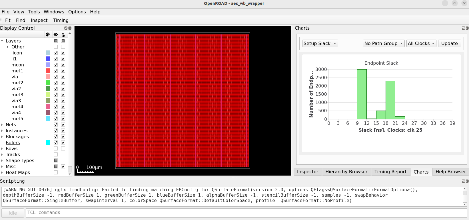
Fig. 8 OpenROAD GUI — Physical Design Inspection Interface
The interface is organised into three primary panels:
Display Control (LHS): Toggle visibility of design layers — Metal layers, Nets, Instances, Blockages. Includes Heatmaps for congestion and power density analysis.
Inspector Window (RHS): Displays properties (coordinates, layer, connectivity) of selected design objects and detailed Timing Reports.
Main Layout View: Central canvas for zooming into pin spacing, track alignment, and cell placement.
Tcl Command Interface
OpenROAD is built on a Tcl-based architecture. Every GUI action can also be executed via the Tcl Console at the bottom of the screen — essential for scripted debugging.
Area Analysis:
report_design_area
Design area 256073 um^2 40% utilization.
Power Analysis:
report_power
Group                  Internal  Switching    Leakage      Total
                          Power      Power      Power      Power (Watts)
----------------------------------------------------------------
Sequential             4.94e-03   2.27e-05   3.68e-08   4.97e-03  63.0%
Combinational          1.62e-03   1.30e-03   8.42e-08   2.92e-03  37.0%
Clock                  0.00e+00   0.00e+00   1.91e-09   1.91e-09   0.0%
Macro                  0.00e+00   0.00e+00   0.00e+00   0.00e+00   0.0%
Pad                    0.00e+00   0.00e+00   0.00e+00   0.00e+00   0.0%
----------------------------------------------------------------
Total                  6.56e-03   1.32e-03   1.23e-07   7.89e-03 100.0%
                          83.2%      16.8%       0.0%
8. Check the Reports
After executing the flow, inspecting the generated reports is essential for verifying design health. These files provide insight into syntax correctness, timing performance, electrical integrity, and power distribution quality.
8.1 Syntax and Linting Checks
The first step of the flow performs a strict linting check. Any critical errors detected at this stage will cause an immediate exit to prevent downstream propagation.
Location:
runs/classic_flow/01-verilator-lint/verilator-lint.logAction: Open this log if the flow crashes at startup. Search for
Errorto identify syntax mismatches or unsupported Verilog constructs.
8.2 Timing and Electrical Summary
The Pre-PnR STA report provides the first snapshot of timing health across all PVT corners, based on the synthesised netlist without physical wire parasitics.
Location:
runs/classic_flow/12-openroad-staprepnr/summary.rpt
┏━━━━━━━━━━━━━━━━━━━━━━┳━━━━━━━━━━┳━━━━━━━━━━┳━━━━━━━━━━┳━━━━━━━━━━┳━━━━━━━━━━━┳━━━━━━━━━━┳━━━━━━━━━━━┳━━━━━━━━━━┳━━━━━━━━━━━┳━━━━━━━━━━┳━━━━━━━━━━━┳━━━━━━━━━━┓
┃                      ┃ Hold     ┃ Reg to   ┃          ┃          ┃ of which  ┃ Setup    ┃           ┃          ┃           ┃ of which ┃           ┃          ┃
┃                      ┃ Worst    ┃ Reg      ┃          ┃ Hold Vio ┃ reg to    ┃ Worst    ┃ Reg to    ┃ Setup    ┃ Setup Vio ┃ reg to   ┃ Max Cap   ┃ Max Slew ┃
┃ Corner/Group         ┃ Slack    ┃ Paths    ┃ Hold TNS ┃ Count    ┃ reg       ┃ Slack    ┃ Reg Paths ┃ TNS      ┃ Count     ┃ reg      ┃ Violatio… ┃ Violati… ┃
┡━━━━━━━━━━━━━━━━━━━━━━╇━━━━━━━━━━╇━━━━━━━━━━╇━━━━━━━━━━╇━━━━━━━━━━╇━━━━━━━━━━━╇━━━━━━━━━━╇━━━━━━━━━━━╇━━━━━━━━━━╇━━━━━━━━━━━╇━━━━━━━━━━╇━━━━━━━━━━━╇━━━━━━━━━━┩
│ Overall              │ -0.7039  │ 0.1242   │ -184.11… │ 1167     │ 0         │ 9.0038   │ 9.7665    │ 0.0000   │ 0         │ 0        │ 36        │ 2377     │
│ nom_tt_025C_1v80     │ -0.6583  │ 0.2630   │ -130.68… │ 389      │ 0         │ 11.3333  │ 17.3576   │ 0.0000   │ 0         │ 0        │ 16        │ 1373     │
│ nom_ss_100C_1v60     │ -0.4039  │ 0.7043   │ -51.3690 │ 389      │ 0         │ 9.0038   │ 9.7665    │ 0.0000   │ 0         │ 0        │ 36        │ 2377     │
│ nom_ff_n40C_1v95     │ -0.7039  │ 0.1242   │ -184.11… │ 389      │ 0         │ 11.2064  │ 20.1298   │ 0.0000   │ 0         │ 0        │ 16        │ 1167     │
└──────────────────────┴──────────┴──────────┴──────────┴──────────┴───────────┴──────────┴───────────┴──────────┴───────────┴──────────┴───────────┴──────────┘
Note
Interpreting this report:
Hold violations are present across all corners. These are expected and normal at the pre-placement stage — they will be systematically resolved during Clock Tree Synthesis (CTS) in Module 2.
Setup violations (Setup Vio Count = 0) are absent. This confirms the AES core’s critical path meets the 40 MHz target clock after applying
DELAY 4synthesis.Max Slew and Max Cap violations vary significantly across corners. Notice that the
nom_ss_100C_1v60(Slow-Slow) corner shows the worst counts — 36 Max Cap and 2,379 Max Slew violations. This is because slower gates and lower voltages produce slower signal transitions and higher effective net loads.Corner coverage: The pre-PnR STA analyses 3 corners. In later stages (post-CTS, post-routing, signoff), the tool expands to 9 corners for a more comprehensive PVT sweep.
Why we set DEFAULT_CORNER: "max_ss_100C_1v60":
The Slow-Slow corner (nom_ss_100C_1v60) produces the highest number of Max Cap and
Max Slew violations by a significant margin. By adding the following to config.json,
we instruct the tool to optimise and repair against this worst-case corner first —
ensuring the design is robust before being validated on other corners:
"DEFAULT_CORNER": "max_ss_100C_1v60"
Add this line to your config.json now. Your complete configuration for Module 2 onward
will be:
{
    "DESIGN_NAME": "aes_wb_wrapper",
    "PDN_MULTILAYER": false,
    "CLOCK_PORT": "wb_clk_i",
    "CLOCK_PERIOD": 25,
    "VERILOG_FILES": [
        "dir::../../../aes/secworks_aes/rtl/*.v",
        "dir::../../verilog/rtl/aes_wb_wrapper.v"
    ],
    "PNR_SDC_FILE": "dir::pnr.sdc",
    "SIGNOFF_SDC_FILE": "dir::signoff.sdc",
    "DEFAULT_CORNER": "max_ss_100C_1v60",
    "FP_CORE_UTIL": 40,
    "RT_MAX_LAYER": "met4",
    "SYNTH_STRATEGY": "DELAY 4"
}
8.3 Detailed Multi-Corner Analysis
For an in-depth timing investigation, navigate to the subdirectories within
12-openroad-staprepnr/. Each subdirectory corresponds to a distinct PVT corner:
Corner Directory |
Description |
|---|---|
|
Fast-Fast corner — best-case (low temperature, high voltage). |
|
Slow-Slow corner — worst-case (high temperature, low voltage). |
|
Typical-Typical corner — nominal operating conditions. |
Each corner directory contains the following critical reports:
File |
Description |
|---|---|
|
Worst Negative Slack for Setup (Max) and Hold (Min) paths. |
|
Total Negative Slack across all failing paths. |
|
Categorised list of all nets and pins failing timing constraints. |
|
Detailed power breakdown: Internal, Switching, and Leakage. |
|
Reports on unconstrained pins, multiple clock domains, or missing arrival times. |
|
Path-by-path reports for the worst-case Setup and Hold paths. |
|
Clock skew analysis across the clock tree. |
|
Raw output log of the OpenROAD STA engine for this corner. |
|
Standard Delay Format file for back-annotation of timing delays. |
8.4 Power Distribution Network (PDN) Integrity
After generating the power grid, verify there are no connectivity issues in the power/ground straps.
VPWR Errors:
runs/classic_flow/19-openroad-generatepdn/VPWR-grid-errors.rptVGND Errors:
runs/classic_flow/19-openroad-generatepdn/VGND-grid-errors.rpt
Warning
If either of these files contains entries, parts of your power grid are not properly connected to the main supply rails. This is a critical electrical integrity issue that must be resolved before proceeding to Placement and Routing.
- RTL
Register-Transfer Level. An abstraction of a digital circuit describing data flow between registers and the logic operations performed on that data.
- GDSII
Graphic Database System II. The standard binary file format used to represent the final physical layout of an integrated circuit, delivered to the foundry for fabrication.
- EDA
Electronic Design Automation. Software tools used to design, verify, and analyze electronic systems, including ICs and PCBs.
- SDC
Synopsys Design Constraints. An industry-standard Tcl-based format for specifying timing and clocking constraints for digital design implementation and analysis.
- PnR
Place and Route. The physical design stage in which synthesized netlist cells are assigned spatial positions (placement) and interconnected with metal wires (routing).
- STA
Static Timing Analysis. A method of validating circuit timing by checking all signal paths against timing constraints without requiring simulation vectors.
- PDN
Power Distribution Network. The network of metal conductors that delivers supply voltage (VDD) and ground (GND) to every cell in the chip.
- PVT
Process, Voltage, Temperature. The three main sources of variation in semiconductor manufacturing that affect circuit performance and are analyzed through multiple design corners.
- DRC
Design Rule Check. A verification step that ensures the physical layout conforms to the foundry’s manufacturing constraints.
- DEF
Design Exchange Format. An ASCII file format describing the physical placement and routing of a chip layout, used for data exchange between EDA tools.
- LEF
Library Exchange Format. A file format describing the physical characteristics of standard cells and macros.
- LVS
Layout vs. Schematic. A physical verification step confirming that the fabricated layout matches the intended circuit schematic.
- SPICE
Simulation Program with Integrated Circuit Emphasis. A general-purpose analog circuit simulator used for electrical verification of layouts.
- PPA
Power, Performance, Area. The three primary optimization metrics in VLSI design, representing a fundamental trade-off space.
- WNS
Worst Negative Slack. The most critical timing violation in a design — the largest magnitude of negative slack across all timing paths.
- TNS
Total Negative Slack. The sum of all negative slack values across failing timing paths.
- CTS
Clock Tree Synthesis. The physical design step that builds a balanced clock distribution network to minimize clock skew across all sequential elements.
- timing closure
The process of iteratively adjusting a design’s implementation until all timing constraints are met across all required PVT corners.